
USI Blog
Top trending topic for the latest innovation technology, application and industry insight.
Search
- 09/07/2026
The Next Frontier in AI Computing: Design and Manufacturing of 1.6T Optical Transceiver Modules

Author: Red Lo, Associate Technical Director, USI R&D Center
The rapid growth of large language models (LLMs) and generative AI is driving unprecedented demand for speed across global data center architectures. While the world focuses on increases in GPU computing power and high-bandwidth memory (HBM) capacity, data centers are confronting a critical bottleneck: the physical limits of network data transmission.
To support cluster computing involving tens of thousands of GPUs, AI data center network topologies are rapidly advancing from mainstream 400G and 800G architectures toward 1.6T. High-speed optical transceiver modules therefore face unprecedented design, validation, and manufacturing challenges. Continued expansion of AI computing capacity depends not only on GPUs, but also on the high-speed optical links connecting them. The ability to integrate high-speed electrical design, thermal management, optical engineering, validation, and advanced manufacturing has become the key competitive differentiator for 1.6T optical modules.
As AI Computing Expands, Network Communication Becomes the New Bottleneck
Through the IEEE 802.3dj Task Force, IEEE is advancing the foundational technologies for 200G/lane, or 200 Gbps per lane, to establish standards for 800G and 1.6T Ethernet. OIF is leading the CEI-224G family of interface projects to enable practical deployment of 224G-class electrical interfaces, a critical technology for connecting 1.6T switch ASICs to optical transceiver modules. Ethernet has established 800G as the primary upgrade target for current AI infrastructure, while 1.6T is positioned as the core backbone for next-generation large-scale clusters and spine networks.
In traditional cloud computing networks, most data traffic is north-south traffic between users and servers. In AI cluster computing, however, intensive parameter synchronization and gradient exchange between GPUs generate massive volumes of east-west traffic. As electrical signals reach the distance and bandwidth limits of conventional copper interconnects, high-speed optical transceiver modules become the vital arteries that keep AI computing systems running.
The transition from 800G to 1.6T involves much more than simply doubling data throughput. In a 1.6T OSFP 2×DR4 or DR8 architecture, for example, the electrical interface reaches 200 Gb/s PAM4 per lane. This exponential increase in data rate introduces three severe physical challenges: signal distortion, high thermal loads, and optical alignment errors.
Design Challenges: The Interplay of SI/PI, Thermal Simulation, and Optical Simulation
Signal Integrity and Power Integrity at Ultra-High Frequencies
Integrating 1.6T data rates into a compact OSFP form factor requires sophisticated simulation and design capabilities during the R&D stage. Once the per-lane data rate exceeds 100 Gb/s, copper traces, vias, and connector pins on the PCB can behave like miniature antennas, causing severe crosstalk, reflections, and high-frequency attenuation.
- SI challenge: Design teams must precisely control impedance and optimize the PCB stack-up. In the 1.6T era, conventional high-speed PCB materials are no longer sufficient. Advanced modified semi-additive process (mSAP) or substrate PCB technologies are required to provide ultra-fine line widths and spacing, together with very low dielectric loss, to maintain signal quality over transmission distances of only a few centimeters.
- PI challenge: The introduction of advanced 3 nm digital signal processors (DSPs) creates extremely high transient current demand. A key aspect of coordinated SI/PI design is ensuring that the power distribution network (PDN) maintains ultra-low ripple during high-speed switching while preventing voltage drops from affecting laser driving and signal detection.
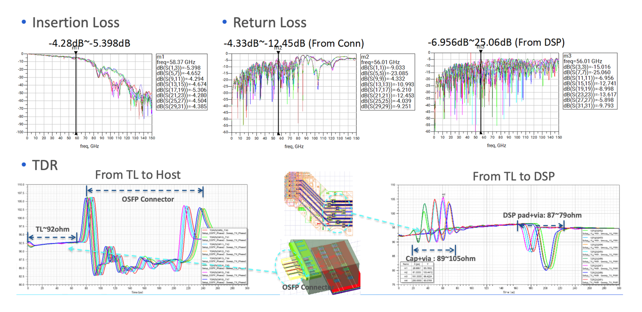
Fig1. SI/PI simulation Example
Thermal Management in a Space-Constrained Module: Thermal Simulation
An 800G optical transceiver consumes approximately 16.5 W, while the higher level of chip integration in a 1.6T optical module greatly increases the thermal load. If the internal module temperature exceeds the industrial-grade threshold of 70°C, the laser’s optical modulation amplitude (OMA) can decline sharply, and its service life may also be shortened.
During the early development stage, advanced thermal simulation software must be used to model airflow and heat conduction around the internal DSP, transimpedance amplifier (TIA), and laser diode. The module structure must then be optimized by improving the enclosure’s heat-sink fin design, selecting thermal interface materials (TIMs) with very high thermal conductivity, and potentially incorporating thermal bridges to direct heat efficiently toward the enclosure. These measures are essential for stable operation of modules consuming 20 W or more.
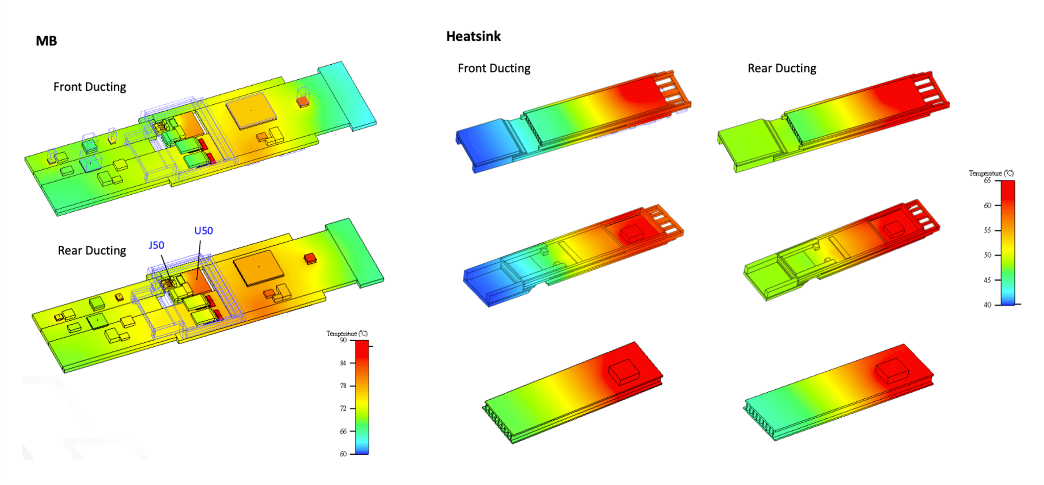
Fig2. Example of Thermal Simulation [ Note: J50: Laser Diode / U50: Photonic Integrated Circuit, PIC ]
Micron-Level Optical Path Control: Optical Simulation
Whether the module uses conventional indium phosphide (InP) lasers or advanced silicon photonics and photonic integrated circuit (PIC) technology, the optical signal travels from the laser through a lens and isolator before being coupled into a fiber array unit (FAU). The allowable alignment tolerance along this optical path is often measured in micrometers (μm) or even nanometers (nm).
Advanced optical simulation tools such as TracePro and Zemax must be used during the design stage to accurately model beam propagation and coupling efficiency. Reflection loss at optical component surfaces and polarization-dependent loss (PDL) should be calculated in advance to prevent minor assembly tolerances from causing insufficient transmit optical power or excessive dispersion. Examples of optical simulation results will be discussed in greater detail in a subsequent article.
Validation Challenges: Rigorous Testing from Optical Eye Diagrams to BERT
No matter how well a high-speed optical transceiver is designed, it must pass rigorous laboratory measurements. Test instruments and methodologies for 800G and 1.6T have entered an entirely new level of complexity. With PAM4, or four-level pulse amplitude modulation, the waveform is no longer represented by simple binary zeros and ones. Instead, four amplitude levels form three eye openings. Even minor signal interference can narrow the eye openings and prevent the receiver from decoding the signal correctly.
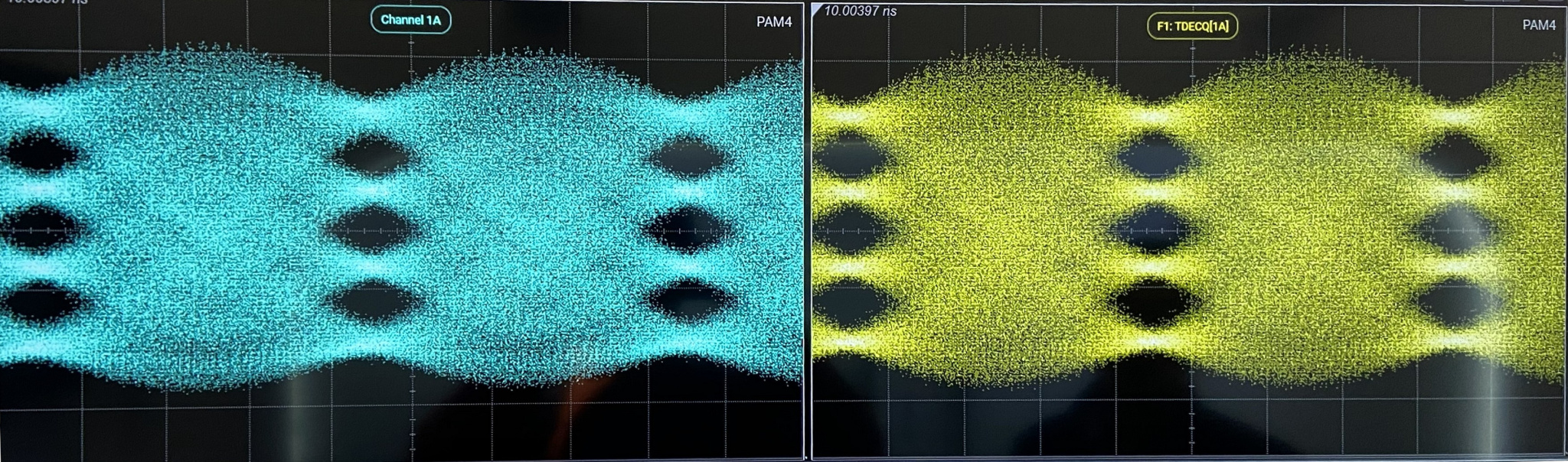
Fig3. Example Optical Eye Diagram for a 1.6T Optical Transceiver Module
To validate the actual performance of a 1.6T optical transceiver module, a professional optical communications laboratory must be equipped with two essential test instruments:
- High-speed sampling oscilloscope: This instrument captures optical eye diagrams at symbol rates of 100 GBaud or higher and accurately measures transmitter and dispersion eye closure quaternary (TDECQ). TDECQ is one of the most critical metrics for evaluating the transmitter quality of a high-speed optical transceiver. A lower value indicates better signal quality. (≤3.4dB)
- Bit error rate tester (BERT): Although high-speed networking chips support forward error correction (FEC), the module’s physical-layer bit error rate before error correction, known as the Pre-FEC BER, must remain within a strict threshold. A BERT transmits billions of pseudorandom binary sequence (PRBS) bits and performs margin and stress testing under boundary conditions involving different temperatures and voltages. This testing helps ensure that the module will operate for tens of thousands of hours without unexpected link interruptions.
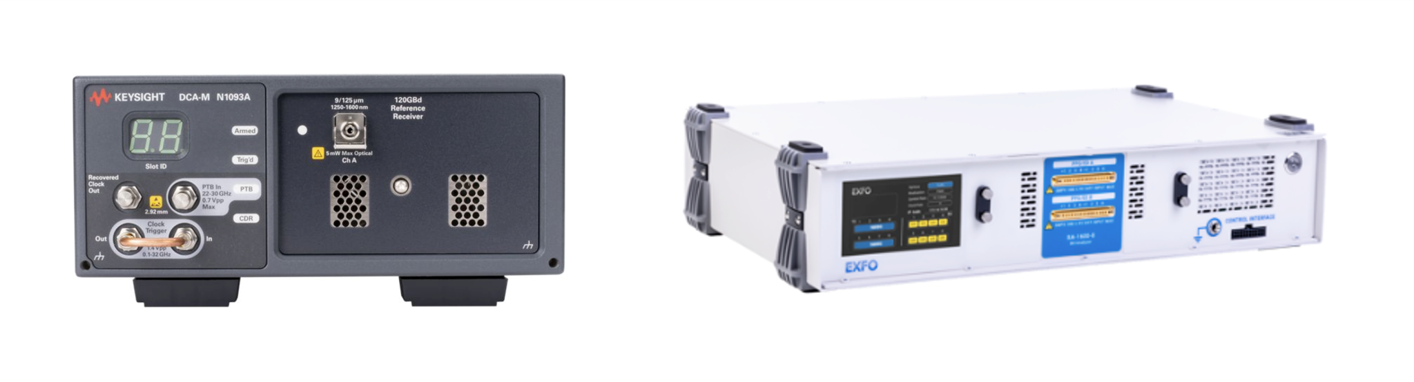
Fig3. Core Validation Equipment: Keysight N1093A 1.6T Oscilloscope (Left) and EXFO BA-1600 BERT (Right)
Manufacturing Challenges: Advanced Packaging and Automated Optical Assembly
As 1.6T products move toward silicon photonics (SiPh) and higher integration density, conventional surface-mount technology (SMT) can no longer fully meet optical transceiver manufacturing requirements. The convergence of electronics manufacturing and advanced semiconductor packaging has therefore become a key competitive arena. Volume production of high-speed optical transceivers depends on a highly integrated manufacturing process.
- High-density SMT and flip-chip packaging: The internal DSP and PIC contain a large number of densely spaced interconnects. Manufacturers must be capable of screening and testing known good dies (KGDs) and must deploy high-precision flip-chip bonders. These capabilities ensure micron-level die placement and bonding accuracy while preventing incomplete solder joints and stress-induced microcracks.
- Die/wire bonding and component integration: In addition to SMT, miniature optoelectronic components inside the module, such as TIAs and PIN photodiodes, require highly precise die and wire bonding. Parasitic inductance must be minimized to preserve high-frequency bandwidth.
- Automated active optical alignment: Optical components, including lasers, lenses, and FAUs, can no longer be assembled solely through fixed mechanical positioning. Active alignment must be used instead. During assembly, the laser is powered on while automated equipment continuously adjusts the component position and monitors the received optical power. Once the maximum-power point, or optimal coupling position, is identified, the adhesive is cured using UV light with the appropriate wavelength, intensity, and exposure time.
- UV adhesive parameter optimization: UV adhesives undergo slight volumetric shrinkage during curing, which is often a major cause of optical path displacement and lower production yield. Precise optimization of curing time, UV intensity, and wavelength is therefore required to achieve both high units per hour (UPH) and high yield in volume production.
As a global leader in electronics design and manufacturing services, USI leverages its strong R&D capabilities to provide industry-leading high-speed SI/PI design, advanced thermal simulation, and optical simulation. For validation, USI operates a professional optical communications laboratory equipped with sampling oscilloscopes and BERT systems, significantly shortening customers’ validation cycles during early-stage product development.
More importantly, USI’s manufacturing capabilities span high-density SMT, KGD flip-chip assembly, die and wire bonding, automated optical alignment, and comprehensive final testing. As AI computing continues to advance in 2026, USI’s end-to-end solution, extending from virtual simulation to volume production, positions the company as a trusted technology and manufacturing partner for global brands and data center leaders building next-generation high-speed AI networks.
Frequently Asked Questions
Q1: Why does 200G/lane increase the PCB design complexity of a 1.6T optical module?
A: At a 200G/lane interface rate, insertion loss, reflections, and crosstalk caused by PCB traces, vias, and connectors become significantly more pronounced. Designers must therefore precisely control impedance, optimize the PCB stack-up, and adopt low-loss dielectric materials and high-density fabrication processes.
Q2: How does power integrity affect the stability of a 1.6T optical transceiver module?
A: A high-speed DSP generates rapidly changing load currents during switching. Excessive ripple or voltage drops in the power distribution network (PDN) can affect the DSP, laser driver, and receiver circuitry. PI simulation is therefore required to optimize power delivery paths and decoupling design.
Q3: What are the primary areas analyzed in thermal simulations of a 1.6T optical module?
A: Thermal simulation primarily analyzes the temperature distribution and heat-transfer paths of the DSP, TIA, laser diode, and photonic integrated circuit (PIC). The results are used to optimize heat-sink fins, thermal interface materials (TIMs), and thermal bridges, reducing the impact of hot spots on optical performance and reliability.
Q4: How does optical simulation reduce coupling loss in a 1.6T optical module?
A: Optical simulation predicts beam propagation and coupling efficiency among the laser, lens, isolator, and fiber array unit (FAU). It also analyzes reflection loss, polarization-dependent loss (PDL), and micron-level assembly tolerances to reduce optical power loss after assembly.
Q5: What signal characteristics are validated by TDECQ and Pre-FEC BER?
A: TDECQ evaluates the optical signal quality of a PAM4 transmitter, with a lower value generally indicating better transmit quality. Pre-FEC BER measures the raw bit error rate before forward error correction and confirms whether the receive link has sufficient decoding margin.
Q6: Why are KGD and flip-chip processes required to manufacture 1.6T optical modules?
A: Known good die (KGD) screening verifies bare-die functionality before assembly, reducing the risk of downstream failures in high-value modules. Flip-chip technology integrates the DSP and PIC through high-density, short interconnects, helping to reduce parasitic effects and improve high-speed signal performance.
Q7: Why do active optical alignment and UV adhesive curing affect volume-production yield?
A: Active optical alignment adjusts component positions in real time while the laser is operating to achieve optimal optical coupling efficiency. If UV adhesive shrinkage occurs during fixation, the optical path may shift. The adhesive material, irradiation wavelength, intensity, and curing time must therefore be precisely controlled.
Search
Recent Articles
-
The Next Frontier in AI Computing: Design and Manufacturing of 1.6T Optical Transceiver Modules
 The Next Frontier in AI Computing: Design and Manufacturing of 1.6T Optical Transceiver Modules
09/07/2026
The Next Frontier in AI Computing: Design and Manufacturing of 1.6T Optical Transceiver Modules
09/07/2026
-
A Key Step in Further Wearable Miniaturization: Selective Encapsulation with Fence + VPE
 A Key Step in Further Wearable Miniaturization: Selective Encapsulation with Fence + VPE
08/17/2026
A Key Step in Further Wearable Miniaturization: Selective Encapsulation with Fence + VPE
08/17/2026
-
Enabling AI at Scale: The Rise of Silicon Photonics and Optical Transceiver
 Enabling AI at Scale: The Rise of Silicon Photonics and Optical Transceiver
08/03/2026
Enabling AI at Scale: The Rise of Silicon Photonics and Optical Transceiver
08/03/2026
-
When AI Learns to “Read”: Using Deep Learning to Tame the False-Alarm Storm on SMT Production Lines
 When AI Learns to “Read”: Using Deep Learning to Tame the False-Alarm Storm on SMT Production Lines
07/13/2026
When AI Learns to “Read”: Using Deep Learning to Tame the False-Alarm Storm on SMT Production Lines
07/13/2026
-
Catching Invisible “Micro-Failures”: Safeguarding SiP Reliability Testing with Daisy Chains
 Catching Invisible “Micro-Failures”: Safeguarding SiP Reliability Testing with Daisy Chains
06/29/2026
Catching Invisible “Micro-Failures”: Safeguarding SiP Reliability Testing with Daisy Chains
06/29/2026
-
The Hidden Rival Inside an EV’s Heart: Cracking the Power-Loss Puzzle with “Physical Modeling”
 The Hidden Rival Inside an EV’s Heart: Cracking the Power-Loss Puzzle with “Physical Modeling”
06/17/2026
The Hidden Rival Inside an EV’s Heart: Cracking the Power-Loss Puzzle with “Physical Modeling”
06/17/2026
-
Behind the MFG. | From "Manufacturing" to "Creation" Ep.2: Innovation Built from Zero to One
 Behind the MFG. | From "Manufacturing" to "Creation" Ep.2: Innovation Built from Zero to One
05/28/2026
Behind the MFG. | From "Manufacturing" to "Creation" Ep.2: Innovation Built from Zero to One
05/28/2026
-
Behind the MFG. | From "Manufacturing" to "Creation" Ep.1: Unveiling USI’s Technological Vanguard
 Behind the MFG. | From "Manufacturing" to "Creation" Ep.1: Unveiling USI’s Technological Vanguard
05/07/2026
Behind the MFG. | From "Manufacturing" to "Creation" Ep.1: Unveiling USI’s Technological Vanguard
05/07/2026
-
Breaking the AI Energy Wall: Power Block and 3D Miniaturization Solutions
 Breaking the AI Energy Wall: Power Block and 3D Miniaturization Solutions
12/31/2025
Breaking the AI Energy Wall: Power Block and 3D Miniaturization Solutions
12/31/2025
-
Mastering Automotive HPC: Defining the "Sweet Spot" of SoMoG Technology
 Mastering Automotive HPC: Defining the "Sweet Spot" of SoMoG Technology
12/15/2025
Mastering Automotive HPC: Defining the "Sweet Spot" of SoMoG Technology
12/15/2025
Keep up with top trending topic
For the latest innovation technology, application
and industry insight.
Subscribe Our Blog
For the latest innovation technology, application
and industry insight.