About
- Press Releases
- 12/06/2021
As Demand for Miniaturization Technology Rises, USI Steps Up Efforts in The Field of Wearable Devices with Innovative SiP Technology

(2021-12-06 Shanghai) This is the ninth year of USI’s entry into the smart wearable module segment and reaching a new level in the development of advanced packaging technology. Double-sided molding and thin-film molding are the latest technologies developed by USI. Double-sided molding optimizes the design of modules. The thin-film molding technology has been introduced to minimize the signal connection lead-out zone, allowing it to work simultaneously on the same substrate side with other molding zones.
Mobile phones have long been the driving force of miniaturization. Nowadays, many fields of application have demonstrated the advantages of miniaturization technology and the demand is especially high in smart wearable devices. SiP (System-in-Package) technology has become a key enabler for highly integrated and miniaturized designs in smart watches, Bluetooth headsets and many new smart wearable products. USI continues to invest in R&D and has made significant breakthroughs in advanced SMT (Surface Mount Technology), molding, new cutting technology (combination of laser cutting and traditional saw blade cutting technology), and thin film sputtering technology.
In terms of SMT capabilities, USI is now able to surface mount components with a smaller pitch based on traditional SMT, achieving a minimum part pitch of 50 microns. At the same time, the company has developed SMT and 3D SMT for single modules, allowing the flexibility of choosing between Panel level or SiP level SMT processes.
Molding technology is a key differentiator in advanced SiP technology compared with traditional packaging processes, which can effectively protect components in high-density packages with small pitches, thereby maximizing space utilization. Based on the traditional molding technology, USI has developed multi-step molding, regional molding, double-sided molding, thin film molding etc. In multi-step molding, the height of the mold can be selected according to the height of the internal packaging components, which reduces molding compound use as well as allows space for designing the product structure. In regional molding, components and signal pins that do not require molding or cannot be molded according to product application requirements shall be exposed outside the molding area. Thus, fulfilling the co-existence of the molded and non-molded packaging on the same side of the PCB.
In traditional packaging, laser technology is often used only for marking. However, USI has further expanded its application areas by developing the use of laser cutting to achieve profiled cutting of modules that meets the design needs of customers and provides greater flexibility for structural design. The laser's high controllability allows the precise cutting of the molding surface while controlling the cutting depth for localized partition shielding.
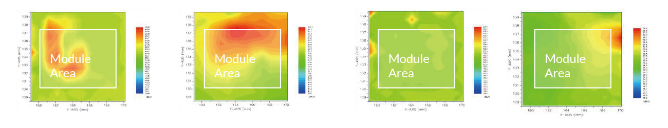
Sputtering shielding is a new process that replaces the traditional iron cover shielding process, providing a better shielding effect, and taking up almost no space. This year, USI has developed an optional sputtering process based on traditional sputtering technology to solve the design problem of the coexistence of electromagnetic shielding zones and non-electromagnetic shielding zones on the same surface of the substrate. The non-electromagnetic shielding zone is protected by sheltering before sputtering, and the sheltering is removed after sputtering. Subsequent SMT of functional components in this zone will be done to realize the separation of functional zones. Currently, USI is also evaluating more efficient electromagnetic shielding technology, atomization spraying process, plasma spraying, vacuum printing, and other development and application processes.
Since 2013, USI has been committed to the miniaturization and highly integrated development of SiP modules related to wearable products, including local partition shielding, selective molding, thin-film molding technology, selective sputtering, and profiled cutting technology, dry ice cleaning technology, 3D metal stencil printing and other new advanced packaging technologies. With the application of more technologies in mass production, USI will continue to invest and innovate in SiP technology.
About USI
USI (SSE: 601231, A constituent of CSI300 Index), Universal Scientific Industrial (Shanghai) Co., Ltd., is a global leader in electronic design and manufacturing as well as a leader in the field of SiP (System-in-Package) modules. USI provides D(MS)2 product services: Design, Manufacturing, Miniaturization, Industrial software and hardware Solutions, and material procurement, logistics and maintenance Services. With Asteelflash, USI has 27 sales, production and service locations across four continents of America, Europe, Asia and Africa, and offers customer diversified products in the sectors of wireless communication, computer and storage, consumer, industrial, medical and automotive electronics worldwide. USI is the subsidiary of ASE Technology Holding Co., Ltd. (TWSE: 3711, NYSE: ASX), the leading provider of semiconductor manufacturing services in assembly and test. To learn more, please visit www.usiglobal.com and engage with us on LinkedIn and YouTube.
Mobile phones have long been the driving force of miniaturization. Nowadays, many fields of application have demonstrated the advantages of miniaturization technology and the demand is especially high in smart wearable devices. SiP (System-in-Package) technology has become a key enabler for highly integrated and miniaturized designs in smart watches, Bluetooth headsets and many new smart wearable products. USI continues to invest in R&D and has made significant breakthroughs in advanced SMT (Surface Mount Technology), molding, new cutting technology (combination of laser cutting and traditional saw blade cutting technology), and thin film sputtering technology.
In terms of SMT capabilities, USI is now able to surface mount components with a smaller pitch based on traditional SMT, achieving a minimum part pitch of 50 microns. At the same time, the company has developed SMT and 3D SMT for single modules, allowing the flexibility of choosing between Panel level or SiP level SMT processes.
Molding technology is a key differentiator in advanced SiP technology compared with traditional packaging processes, which can effectively protect components in high-density packages with small pitches, thereby maximizing space utilization. Based on the traditional molding technology, USI has developed multi-step molding, regional molding, double-sided molding, thin film molding etc. In multi-step molding, the height of the mold can be selected according to the height of the internal packaging components, which reduces molding compound use as well as allows space for designing the product structure. In regional molding, components and signal pins that do not require molding or cannot be molded according to product application requirements shall be exposed outside the molding area. Thus, fulfilling the co-existence of the molded and non-molded packaging on the same side of the PCB.
In traditional packaging, laser technology is often used only for marking. However, USI has further expanded its application areas by developing the use of laser cutting to achieve profiled cutting of modules that meets the design needs of customers and provides greater flexibility for structural design. The laser's high controllability allows the precise cutting of the molding surface while controlling the cutting depth for localized partition shielding.
Sputtering shielding is a new process that replaces the traditional iron cover shielding process, providing a better shielding effect, and taking up almost no space. This year, USI has developed an optional sputtering process based on traditional sputtering technology to solve the design problem of the coexistence of electromagnetic shielding zones and non-electromagnetic shielding zones on the same surface of the substrate. The non-electromagnetic shielding zone is protected by sheltering before sputtering, and the sheltering is removed after sputtering. Subsequent SMT of functional components in this zone will be done to realize the separation of functional zones. Currently, USI is also evaluating more efficient electromagnetic shielding technology, atomization spraying process, plasma spraying, vacuum printing, and other development and application processes.
Since 2013, USI has been committed to the miniaturization and highly integrated development of SiP modules related to wearable products, including local partition shielding, selective molding, thin-film molding technology, selective sputtering, and profiled cutting technology, dry ice cleaning technology, 3D metal stencil printing and other new advanced packaging technologies. With the application of more technologies in mass production, USI will continue to invest and innovate in SiP technology.
About USI
USI (SSE: 601231, A constituent of CSI300 Index), Universal Scientific Industrial (Shanghai) Co., Ltd., is a global leader in electronic design and manufacturing as well as a leader in the field of SiP (System-in-Package) modules. USI provides D(MS)2 product services: Design, Manufacturing, Miniaturization, Industrial software and hardware Solutions, and material procurement, logistics and maintenance Services. With Asteelflash, USI has 27 sales, production and service locations across four continents of America, Europe, Asia and Africa, and offers customer diversified products in the sectors of wireless communication, computer and storage, consumer, industrial, medical and automotive electronics worldwide. USI is the subsidiary of ASE Technology Holding Co., Ltd. (TWSE: 3711, NYSE: ASX), the leading provider of semiconductor manufacturing services in assembly and test. To learn more, please visit www.usiglobal.com and engage with us on LinkedIn and YouTube.