Miniaturization becomes much more important, especially for mobile devices, Internet of Things (IoT) and wearable electronics. By integration of these miniaturization solutions, most electronic systems can reduce size to meet market requirements. USI's miniaturization capability is combined with circuit miniaturization to system function integration design. We use the advanced SiP (System-in-Package) technology to achieve the advantage of heterogeneous integration in small modules.
The benefits of SiP :
- Size (XY) reduction to have more space for battery and integrate more functions
- Reduce thickness (Z) and weight for stylish ID design
- Reduce final assembly, test & pack difficulty
- Improve signal integrity
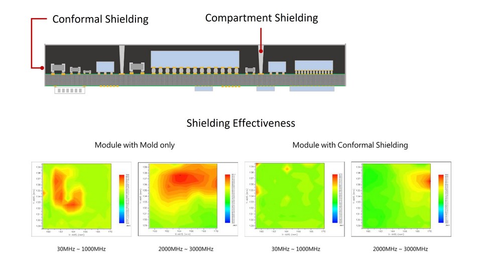
- EMI shielding interference
- Speed up development
- Better reliability-humidity and mechanical
- Better logistics and inventory management
USI has been committed to the miniaturization and highly integrated development of SiP modules related to wearable products, including local partition shielding, selective molding, thin-film molding technology, selective sputtering, and profiled cutting technology, dry ice cleaning technology, 3D metal stencil printing and other new advanced packaging technologies. Double-sided molding and thin-film molding are the latest technologies developed by USI. Double-sided molding optimizes the design of modules. The thin-film molding technology has been introduced to minimize the signal connection lead-out zone, allowing it to work simultaneously on the same substrate side with other molding zones.

SiP Technologies
Shielding
-

Shielding


