About
- Media Highlights
- 06/13/2017
Integrating Group Resources: USI is Becoming the Technology Leader of SiP/SiM Market (DIGITIMES)
Senior Vice President, Mr. Frank Wu
(DIGITIMES 06/13/2017) With the rapid development of mobile products and wearable devices, the miniaturization and systemization of functional modules have become a trend, bringing about brand new development opportunities for Universal Scientific Industrial (Shanghai) Co., Ltd. (USI). The company has endeavored itself in the market of SiP/SiM for a long time. Especially after its integration with the resources of ASE Group, USI has firmly occupied the leading status in the market and is utilizing its ability in miniaturizing systematic products as its weapon when competing in the new generation mobile smart device market. At the same time, USI is also dedicating itself to the development of comprehensive problem-solving solutions that can integrate the capabilities of both software and hardware and thus create higher added value with its differentiated advantages.
USI has Endeavored in the Market of SiP/SiM for a Long Time
Universal Scientific Industrial (Shanghai) Co., Ltd., the predecessor of Universal Scientific Industrial Co., Ltd., was officially incorporated into ASE Group in 2010. Senior Vice President, Frank Wu, of USI stated that, Universal Scientific Industrial Co., Ltd. has already released thick film hybrid IC products back in 1976 when the company was first founded. From today’s perspective, it was actually the predecessor of the SiP (System-in-Package). Although the company later gradually transferred its focus on PCBA (PrintedCircuit Board Assembly) products, it did not let go off its thick film hybrid IC technologies, which was the reason why it could rapidly enter the SiP field.
However, there are still differences between SiP and thick film hybrid IC. Frank Wu explained that there are two major differences: one is that the base is changed from ceramics to substrates, and the other one is the new molding technology. The former one was mainly due to material attribute, causing substrates to have problems such as easily becoming damp and bent during the manufacturing process. As for the latter, they encountered knowledge insufficiency regarding fluid mechanics and impurity removal, and the challenges of irregular shape molding and electromagnetic shielding.
Senior Director, David Lu, on the R&D Department of USI further pointed out that, SiP/SiM products of USI integrate high density SMT (surface mount technology) with packing technologies to further miniaturize the module. When compared with conventional SiM products, its greatest difference is the introduction of molding and sputtering manufacturing process. A metal layer was added through sputtering after molding and solidifying in order to replace traditional metal cases to achieve the effect of electromagnetic shielding.
Given that thicknesses of metal cases are usually around 100um and the thickness of sputtering is only a few micrometers, it is a great progress for the thickness to be reduced by 100um for miniature modules. In addition to that, given that the upper and side gaps between molding and components are also reduced, it can further reduce the thickness.
USI started introducing single-sided molding and sputtering technology from 2010 and have shipped Wi-Fi modules in great number. This is an evident benefit due to combining the packing technology of AGE Group and is an important key to why USI can perform outstandingly in the Wi-Fi miniaturized module market in recent years. With the constant development of packaging technologies, USI will integrate other technologies such as PoP, MOM and others to continuously pursue the development of SiP including Micro SSD.
Frank Wu stated that AGE Group itself is a company that specialized in package test technologies and possesses more experience on different scenarios of packaging. Therefore, with the experience of AGE Group, it greatly reduces USI in going the long way when introducing new manufacturing processes. From the selection of machines and facilities, the adjustment of machine parameter configuration, and problem analysis and resolutions, ASE Group has helped USI greatly. However, as the complexity of SiP gradually enhances and more components are required, they are starting to face scenarios that even ASE Group had never faced before. This is when the hard work of both sides starts to take place. By sharing their know-how with one another, they can each seek improvements and cooperate together to solve problems, so that the greatest synergy of the group can be demonstrated.
Constant Development of Miniaturizing Technology
Speaking of the market development of miniaturization, Frank Wu pointed out that the demands for miniaturizing technology always exist and the most evident example is computers. Fifty years ago, a computer took up a whole room of space and you need an air conditioner to cool it down. Nowadays, an ultra-thin notebook PC not only greatly reduces in its size, but also has way better operation capabilities than those old computers. Now with the vigorous development of mobile electronic products, consumers desire higher quality and better efficiency. Therefore, developers have to constantly pursue greater functions in smaller areas, making miniaturization the key to SiP.
He stressed that miniaturizing technology is basically integrating two or more dies into one module, making it equipped with specific system functions. Therefore, regarding different product markets, the emphasis of miniaturizing technology also differs. For example, USI is skilled in wireless module products, so its major considerations when designing them are their form factors, costs, and signal shielding. For wearable devices, their emphasis is low power, cost, and high defect-free rate packaging. For vehicle electronics, reliability, high power, testability, and form factors are their primary emphasis. If USI wants to enter other product markets in the future, it has to understand their previous features and further improve upon its own R&D skills.
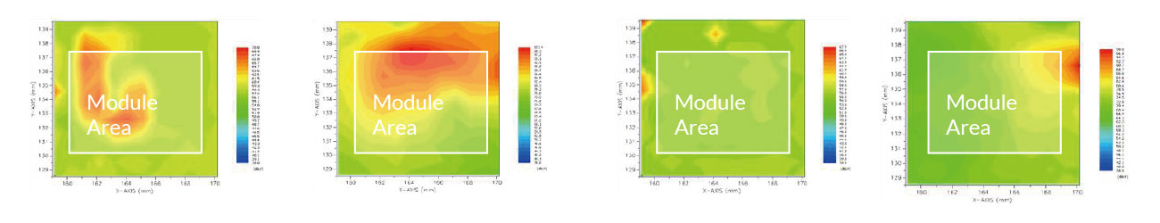
Regarding SiP/SiM technology, the constant miniaturizing of module size XZY is USI’s number one mission and the major challenge to overcome. After successfully establishing its single-sided molding and sputtering technology, USI started to devote itself in the technological development of double-sided molding in 2015. This was mainly due to the fact that customers wanted their Wi-Fi modules to be further miniaturized in size but also had a larger tolerance for their height.
However, given that the market is having more demand regarding the size of miniaturized modules; USI now is capable of shipping a large number of single-sided molding and sputtering products. In addition, the development of comprehensive double-sided molding and sputtering products is scheduled to be completed in 2017. By then, it is estimated that the thickness of Wi-Fi modules can be decreased to merely 0.8mm, making device products thinner than they are now. In order to realize this goal, the RF shielding, heat dissipation and other problems caused by double-sided molding and sputtering must be overcome one by one.
As a matter of fact, regarding wearable devices and products, USI has used double-sided molding technology to integrate more than 500 components on a 12-layer PCB plate within the area of the size of a watch. Given that its shape is irregular and different components have different heights, besides the increase of difficulty when controlling the mold flow uniformity of molding, how to solve the mutual interference of radio-frequency signal within that small area is also another challenge. The successful development of such product fully demonstrates the outstanding technological strength of USI.
Emerging Market Demand Challenges and Business Opportunities Co-exist
Frank Wu stated that the reasons why miniaturizing technologies are broadly discussed recently is mainly because it not only costs cheaper than SoCs (System on Chip), it can also hasten the product’s release time, which are both vital features to consumer electronic products. Miniaturizing technology can be utilized in products such as smart phones, tablet PCs, wearable devices (including medical products), high efficiency video game consoles, notebook PCs, internet & communication facilities, vehicle electronics, and even IoT related applications, such as smart home, energy products, industrial automation, and others.
However, although the market of miniaturization has a bright future, there are still challenges to overcome now, especially regarding costs and development timetable. Frank Wu pointed out given that molding, sputtering and shielding technologies from packaging field are introduced into the manufacturing process of these products, the consequent costs have yet to allow the market to completely accept them. Nevertheless, it is the development trend of future products and he believed that after a while of time, market acceptance will largely increase and allow them to achieve scale economy. By then, cost will no longer be a problem in developing miniaturizing technology.
In addition to that, the design of miniaturized products will integrate several ICs. Given that the development timetable and product design on chips from each IC manufacturers differ, besides having to wait for the complete development of new chips, a certain amount of time is required to integrate chips from different manufacturers. Therefore, the development timetable of miniaturized products is yet to completely satisfy market demands. However, by conducting strategic cooperation with semiconductor manufacturers in simultaneous development, this problem can be solved and shorten the development timetable of these products.
Looking into the future, USI expects to become a technology leader and occupies the number one spot in SiP industry. Frank Wu stressed that regarding technology, it will integrate ASE Group’s latest packaging manufacturing process and technology to strengthen their software and problem-solving solution capabilities. In addition to that, USI also has advantages in product and module designing, abundant experiences after years of manufacturing service, and customer relationships, thus it is confident in providing customers with comprehensive SiP product design, manufacturing process and after-sale service. At the same time, vertical & horizontal integration with the supply chain and conducting strategic alliance are also major parts of the agenda for future development. He optimistically sees the achievement this goal as within sight.