
USI Blog
Top trending topic for the latest innovation technology, application and industry insight.
Search
- 09/21/2026
Inside 1.6T Optical Transceivers: How Optical Simulation and Coupling Shape Performance and Yield

In the third article of this series, USI turns to the most precise, yet often overlooked, core of optical design. From optical simulation to optical coupling, we explain why micron-level control of the optical path is often the final factor determining the yield, cost, and manufacturability of 1.6T optical transceivers.
Two Approaches to Optical Simulation: Wave Optics and Ray Tracing
Optical simulation software is widely used in optical product design. For example, imaging software helps camera-lens designers evaluate optical performance, including resolution, Seidel aberrations, chromatic aberration and other key imaging characteristics. In a 1.6T optical transceiver, even a micron-level component offset can reduce coupling efficiency, lower transmit power, or degrade receiver sensitivity.
Optical simulation is therefore more than a design aid. It is essential to manufacturability and production yield. As optical communications move further into optoelectronic semiconductors, designers select software according to product needs. These tools fall into two main categories: wave optics and geometric optics.
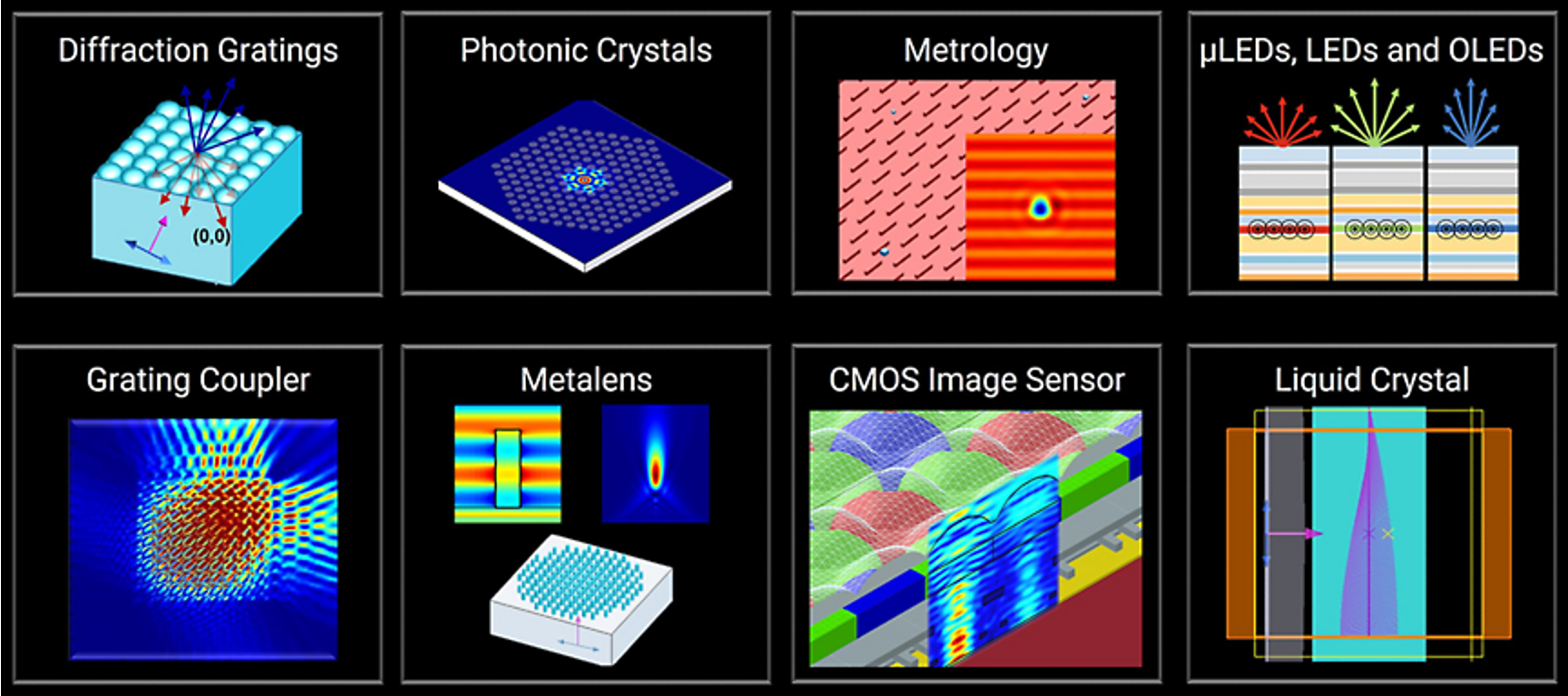
Figure 1. Wave-optics methods such as FDTD are commonly used to analyze photonic microstructures, including diffraction gratings, photonic crystals, and grating couplers.
Wave-Optics Software: Lumerical and RSoft
Wave-optics tools solve Maxwell’s equations to analyze electromagnetic-wave propagation and optical-field distributions. A common method is finite-difference time-domain (FDTD), which models scattering, diffraction, interference, reflection, absorption, and transmission in microstructures. It is widely used to design photonic integrated circuits (PICs)[a]. Common tools include Lumerical FDTD and RSoft FullWAVE.
Because FDTD is computationally intensive and time-consuming, other wave-optics tools serve specific needs. Lumerical MODE and RSoft FemSIM can analyze waveguides and cross-sectional modes, while Lumerical INTERCONNECT and RSoft Photonic Device Compiler support PIC architecture simulation and design.
Geometric-Optics Software: Zemax OpticStudio, CODE V, Speos, LightTools, and TracePro
These tools model light as geometric rays and disregard wave effects such as interference and diffraction. They rely on four core assumptions and laws:
- Light travels in straight lines through a homogeneous medium.
- Rays propagate independently and do not affect one another when they intersect.
- Law of reflection: At an interface, the angle of reflection equals the angle of incidence. The incident ray, reflected ray, and normal lie in the same plane.
- Law of refraction (Snell’s Law): Light bends when entering another medium because its speed changes. The equation is n₁ sin A₁ = n₂ sin A₂.
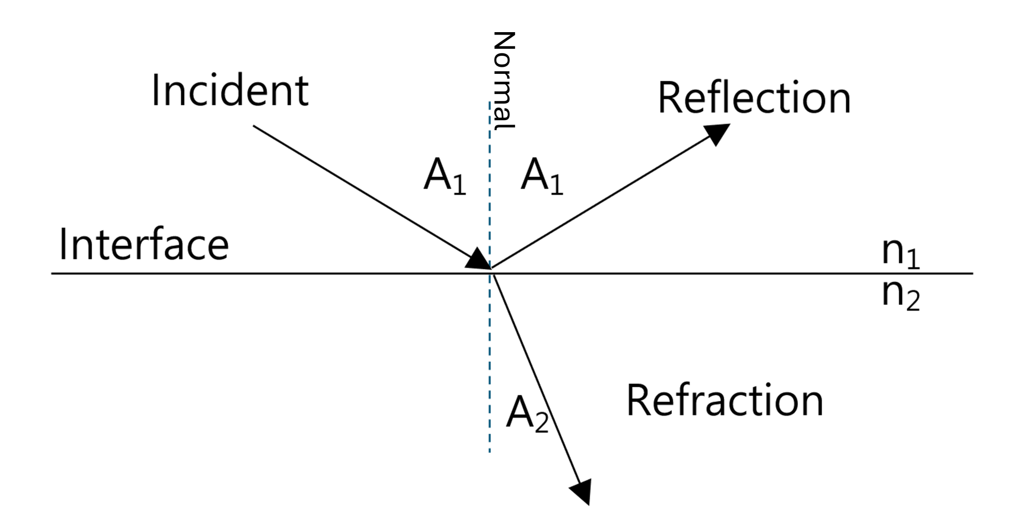
 Figure 2. Conceptual illustration of the laws of refraction and reflection.
 Sequential and Non-Sequential Ray Tracing: Two Simulation Methodologies
Geometric-optics simulation can be divided into sequential and non-sequential ray tracing. Sequential tools include Zemax OpticStudio[b], CODE V, and OSLO. Non-sequential tools include Speos, LightTools, and TracePro.
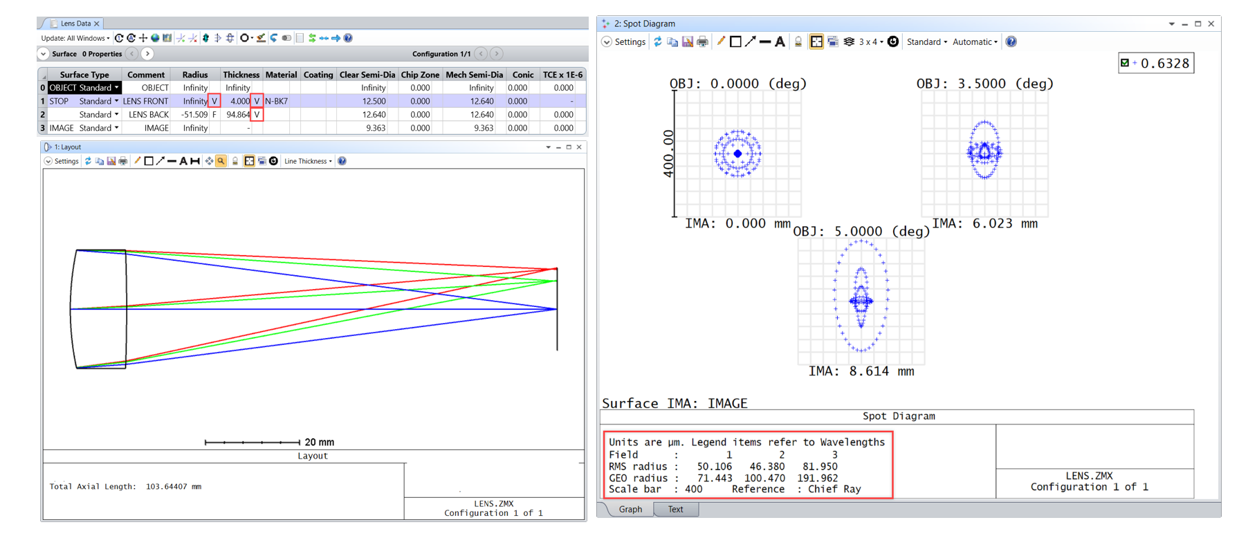
Figure 3. Zemax OpticStudio example: Sequential ray tracing is fast and efficient for optimization, making it well suited to lens and imaging-system design.
- Sequential Ray Tracing: These tools use the paraxial approximation to simplify calculations and define the order in which rays pass through optical surfaces. Refraction and reflection are analyzed in this fixed sequence.
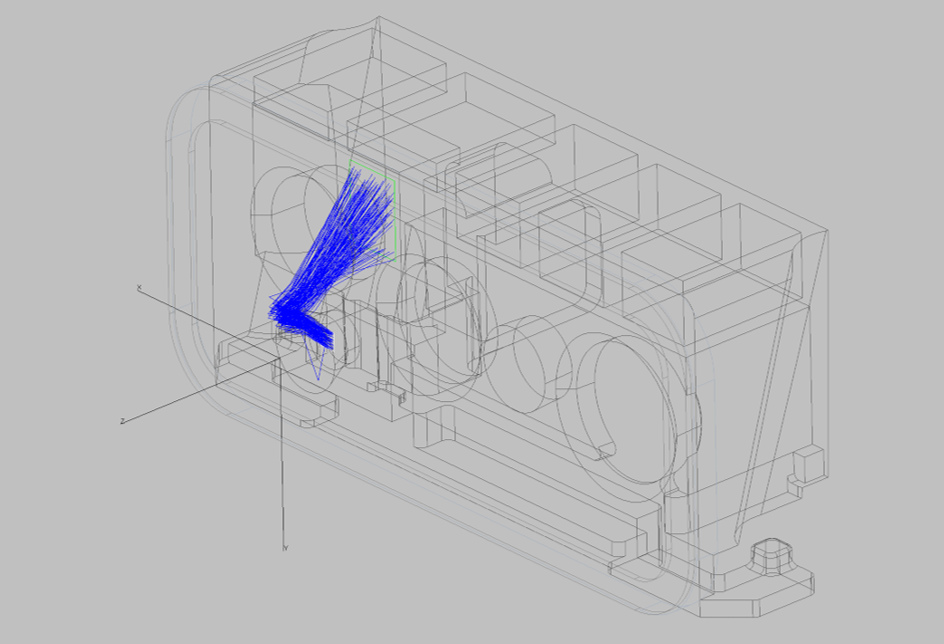
Figure 4. TracePro example: Non-sequential ray tracing more closely represents real optical behavior and is often used to analyze stray light and ghost images.
- Non-Sequential Ray Tracing: These tools do not constrain ray paths. Based on actual geometry, they calculate energy distribution through reflection, refraction, and absorption. Rays propagate repeatedly until they reach a detector, leave the system, or fall below a set energy threshold. Optical-chip designers rely heavily on wave-optics simulation because device structures are typically measured in micrometers or even nanometers. EMS providers, by contrast, generally design larger optical components and modules, where light can be modeled as rays.
Optical-chip designers rely heavily on wave-optics simulation because device structures are typically measured in micrometers or even nanometers, where diffraction, interference, and modal distributions materially affect performance. EMS providers, by contrast, generally design larger optical components and modules, where light can be modeled as rays. They therefore use geometric-optics software more often for product development and optimization.
Optical Transceiver Design: Transmitter Coupling and Receiver Focusing
In USI’s optical transceiver development, geometric-optics software is the primary tool for optical-path analysis. At the transmitter (Tx), simulations focus on coupling efficiency between the optical signal and fiber. At the receiver (Rx), they optimize focusing so the signal reaches the photodetector (PD) accurately.
Optical Transceiver Design: Transmitter Coupling and Receiver Focusing
In USI’s optical transceiver development, geometric-optics software is the primary tool for optical-path analysis. At the transmitter (Tx), simulations focus on coupling efficiency between the optical signal and fiber. At the receiver (Rx), they optimize focusing so the signal reaches the photodetector (PD) accurately.
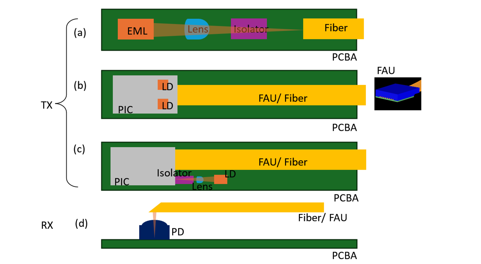
Figure 5. Optical architecture and ray-tracing simulation for the optical transceiver’s transmitter (Tx) and receiver (Rx), including EML/PIC coupling schemes and receiver focusing corresponding to (a)–(d).
Figures 5(a), 5(b), and 5(c) show top views of transmitters using different architectures; Figure 5(d) shows a side view of the receiver. (a) An EML scheme with one optical path. (b) A PIC with an integrated laser diode (LD); because a PIC typically contains multiple optical channels, it uses an FAU. (c) A PIC without embedded LD. (d) Receiver architecture: one PD with one fiber; a PD array would use an FAU.
Transmitter (Tx): EML and Silicon-Photonics (PIC) Coupling Schemes
Two main transmitter approaches are available: an electro-absorption modulated laser (EML) or a PIC-based design. Each requires coupling analysis from the light source to the fiber, from the source to the chip, or from the chip to the fiber.
- EML Coupling Design: As shown in Figure 5(a), at least one lens and an isolator typically couple laser light into the fiber. Simulation software helps design the lens, calculate coupling efficiency, and analyze tolerances to estimate system loss and manufacturing feasibility.[c] Figure 6 provides details.
- PIC Design: Two chip configurations are available. One packages the laser within the PIC, as shown in Figure 5(b); the other provides a standalone PIC that requires an external laser, as shown in Figure 5(c). For an integrated-laser PIC, downstream module makers follow the PIC design guide and the chip supplier’s recommended fiber array unit (FAU) specifications, with only minor adjustments for system dimensions. For an external-laser PIC, designers must couple the laser into the PIC. The method resembles the EML approach, except that the fiber is replaced by an on-chip waveguide and coupling calculations must address mode matching. At the PIC output, designers follow the same design guide to size the FAU interface.
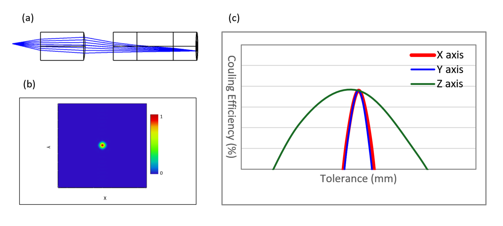
Figure 6. Laser-to-fiber coupling simulation. (a) Component architecture and ray diagram. (b) Irradiance map. (c) Tolerance analysis.
Receiver (Rx): Angled FAU and Precision Focusing
At the receiver, the optical signal exits the fiber and is focused through a lens onto the photodetector chip, as shown in Figure 5(d). Space constraints require an angled FAU facet to redirect light from horizontal to vertical. A lens on the PD surface then focuses the light onto the active area. Optical simulation determines the fiber-facet angle, estimates coupling efficiency, and calculates allowable tolerances, as shown in Figure 7.
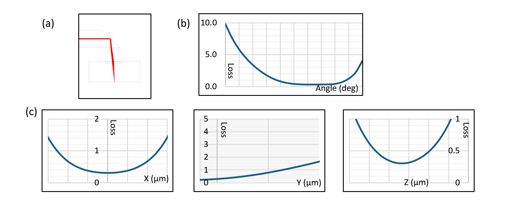
Figure 7. Receiver optical simulation. (a) Component architecture and ray diagram. (b) Fiber angle versus loss. (c) FAU positional tolerance analysis.
From Design to Production: USI and EugenLight’s End-to-End Capabilities
For investors and prospective customers, optical simulation and coupling design matter because they directly affect yield, cost, and lead time. As per-lane rates advance to 200 Gb/s PAM4 and modules scale to 1.6T and beyond, micron-level coupling errors can produce significant power loss and yield degradation.
USI and EugenLight have established design and development experience for both the transmitter and receiver sides of optical transceivers, with R&D achievements spanning optical transceiver modules and external laser small form-factor pluggable (ELSFP) modules. Together, they can provide an end-to-end optical communications solution covering simulation, coupling design, validation, and mass production. This helps global brands and data center operators move faster in the race for AI optical interconnects.
Learn more about USI Optical Products Catalog and Optical Transceivers Profile
Notes
[a] Most PICs use silicon as the base material and are therefore commonly described as silicon photonics.
[b] Zemax OpticStudio includes non-sequential ray tracing, although sequential ray tracing remains its popular user mode.
[c] Replacing the light source with a distributed feedback (DFB) laser creates an external laser small form-factor pluggable module. An EML carries a modulated signal, while a DFB laser provides continuous-wave (CW) light.
Frequently Asked Questions (FAQ)
Q1: What is optical coupling, and why does coupling efficiency affect optical-module yield?
A: Optical coupling transfers optical signals efficiently among lasers, lenses, PICs, fibers, and photodetectors...
Q2: How do wave-optics and geometric-optics simulations differ, and which should optical-module designers use?
A: Wave optics models diffraction, interference, polarization, and modal propagation, while geometric optics uses ray tracing to analyze propagation paths...
Q3: How do sequential and non-sequential ray tracing differ?
A: Sequential ray tracing follows a predefined surface order, while non-sequential ray tracing imposes no fixed object order...
Q4: How does optical coupling differ between discrete EML optics and integrated silicon-photonics architectures?
A: A discrete EML architecture typically uses lenses and isolators to couple light into a fiber, while a silicon-photonics architecture must couple the laser source, PIC interface, and FAU.
Q5: How do FAU angle, pitch, and positional tolerances affect optical coupling efficiency?
A: Out-of-tolerance position, angle, end-face geometry, or channel pitch can increase coupling loss or cause inconsistent channel performance.
Q6: How can optical-simulation results be translated into a production-ready coupling process?
A: Optical simulation defines positional, angular, and dimensional tolerances, which can then be converted into fixture designs, alignment parameters, curing conditions, and automated manufacturing specifications.
Q1: What is optical coupling, and why does coupling efficiency affect optical-module yield?
A: Optical coupling transfers optical signals efficiently among lasers, lenses, PICs, fibers, and photodetectors...
Q2: How do wave-optics and geometric-optics simulations differ, and which should optical-module designers use?
A: Wave optics models diffraction, interference, polarization, and modal propagation, while geometric optics uses ray tracing to analyze propagation paths...
Q3: How do sequential and non-sequential ray tracing differ?
A: Sequential ray tracing follows a predefined surface order, while non-sequential ray tracing imposes no fixed object order...
Q4: How does optical coupling differ between discrete EML optics and integrated silicon-photonics architectures?
A: A discrete EML architecture typically uses lenses and isolators to couple light into a fiber, while a silicon-photonics architecture must couple the laser source, PIC interface, and FAU.
Q5: How do FAU angle, pitch, and positional tolerances affect optical coupling efficiency?
A: Out-of-tolerance position, angle, end-face geometry, or channel pitch can increase coupling loss or cause inconsistent channel performance.
Q6: How can optical-simulation results be translated into a production-ready coupling process?
A: Optical simulation defines positional, angular, and dimensional tolerances, which can then be converted into fixture designs, alignment parameters, curing conditions, and automated manufacturing specifications.
Search
Recent Articles
-
From Untestable to Precisely Tested: Cracking the High-Density ICT Challenge
 From Untestable to Precisely Tested: Cracking the High-Density ICT Challenge
10/16/2026
From Untestable to Precisely Tested: Cracking the High-Density ICT Challenge
10/16/2026
-
Inside 1.6T Optical Transceivers: How Optical Simulation and Coupling Shape Performance and Yield
 Inside 1.6T Optical Transceivers: How Optical Simulation and Coupling Shape Performance and Yield
09/21/2026
Inside 1.6T Optical Transceivers: How Optical Simulation and Coupling Shape Performance and Yield
09/21/2026
-
The Next Frontier in AI Computing: Design and Manufacturing of 1.6T Optical Transceiver Modules
 The Next Frontier in AI Computing: Design and Manufacturing of 1.6T Optical Transceiver Modules
09/07/2026
The Next Frontier in AI Computing: Design and Manufacturing of 1.6T Optical Transceiver Modules
09/07/2026
-
A Key Step in Further Wearable Miniaturization: Selective Encapsulation with Fence + VPE
 A Key Step in Further Wearable Miniaturization: Selective Encapsulation with Fence + VPE
08/17/2026
A Key Step in Further Wearable Miniaturization: Selective Encapsulation with Fence + VPE
08/17/2026
-
Enabling AI at Scale: The Rise of Silicon Photonics and Optical Transceiver
 Enabling AI at Scale: The Rise of Silicon Photonics and Optical Transceiver
08/03/2026
Enabling AI at Scale: The Rise of Silicon Photonics and Optical Transceiver
08/03/2026
-
When AI Learns to “Read”: Using Deep Learning to Tame the False-Alarm Storm on SMT Production Lines
 When AI Learns to “Read”: Using Deep Learning to Tame the False-Alarm Storm on SMT Production Lines
07/13/2026
When AI Learns to “Read”: Using Deep Learning to Tame the False-Alarm Storm on SMT Production Lines
07/13/2026
-
Catching Invisible “Micro-Failures”: Safeguarding SiP Reliability Testing with Daisy Chains
 Catching Invisible “Micro-Failures”: Safeguarding SiP Reliability Testing with Daisy Chains
06/29/2026
Catching Invisible “Micro-Failures”: Safeguarding SiP Reliability Testing with Daisy Chains
06/29/2026
-
The Hidden Rival Inside an EV’s Heart: Cracking the Power-Loss Puzzle with “Physical Modeling”
 The Hidden Rival Inside an EV’s Heart: Cracking the Power-Loss Puzzle with “Physical Modeling”
06/17/2026
The Hidden Rival Inside an EV’s Heart: Cracking the Power-Loss Puzzle with “Physical Modeling”
06/17/2026
-
Behind the MFG. | From "Manufacturing" to "Creation" Ep.2: Innovation Built from Zero to One
 Behind the MFG. | From "Manufacturing" to "Creation" Ep.2: Innovation Built from Zero to One
05/28/2026
Behind the MFG. | From "Manufacturing" to "Creation" Ep.2: Innovation Built from Zero to One
05/28/2026
-
Behind the MFG. | From "Manufacturing" to "Creation" Ep.1: Unveiling USI’s Technological Vanguard
 Behind the MFG. | From "Manufacturing" to "Creation" Ep.1: Unveiling USI’s Technological Vanguard
05/07/2026
Behind the MFG. | From "Manufacturing" to "Creation" Ep.1: Unveiling USI’s Technological Vanguard
05/07/2026
Keep up with top trending topic
For the latest innovation technology, application
and industry insight.
Subscribe Our Blog
For the latest innovation technology, application
and industry insight.