USI Blog
Top trending topic for the latest innovation technology, application and industry insight.
Search
- 12/31/2025
Breaking the AI Energy Wall: Power Block and 3D Miniaturization Solutions

Speaker: Dr. Li-Cheng Shen, Director, Miniaturization Competence Center (MCC), USI
Recently at the IMPACT 2025 conference, Dr. Li Cheng Shen of USI was invited to be the keynote speaker at the IMPACT 2025, sharing our latest technology roadmap for High-Performance Computing (HPC). Facing the immense hunger for compute power in AI servers, we believe that "Power Delivery" is no longer a supporting actor but the critical fuel determining the speed of AI development. This article will provide an in-depth analysis of how USI overcome physical space limitations and achieve the high-performance power solutions required for next-generation AI infrastructure through advanced modularization and miniaturization process technologies.
Why Has "Power Delivery" Become the Invisible Ceiling for AI Development?
In the era of Generative AI, demand for compute power is exploding exponentially, leading to a sharp rise in the Thermal Design Power (TDP) of chips. While many focus on computing speed, for the industry, understanding "Energy Eagerness" is the first step in grasping hardware trends. According to our analysis, the power consumption trends for mainstream GPUs are as follows:
- Nvidia Architecture: From the H100’s 700W (SXM) to the next-generation Blackwell (B200) at 1,200W, and the future Rubin platform expected to exceed 2,000W, power demand has multiplied in just a few years .
- AMD & Intel Architectures: A similarly steep upward curve is evident, with the AMD MI355X projected to reach 1,400W and the Intel Gaudi 3 increasing significantly to 900W .
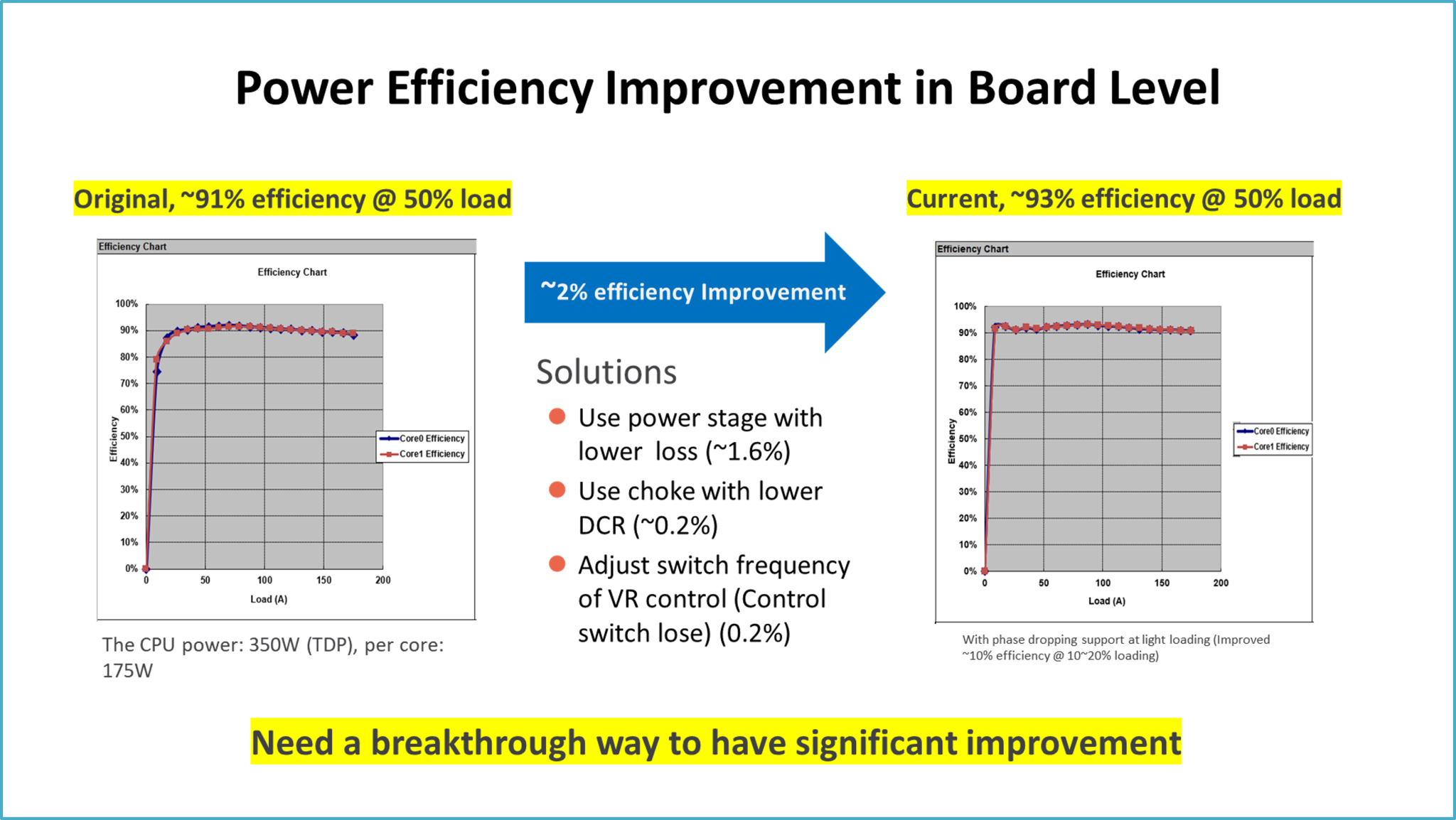
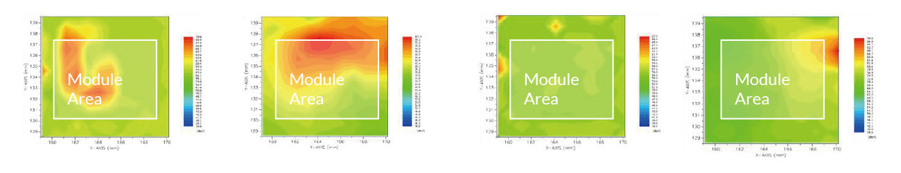
Fig 1. Conventional Power Efficiency Improvement in Board Level
Traditionally, swapping in lower-loss components (such as Power Stages or inductors) only yields an efficiency gain of about 2%. Facing doubled power demands, we must seek breakthrough innovations to have significant improvement.
How to Implement "Vertical Power Delivery"
To meet the demands of space and efficiency simultaneously, the shift in power architecture from lateral to vertical has become an industry consensus. USI's R&D focuses on leveraging packaging and modularization technologies to facilitate the practical implementation of this architectural transformation.
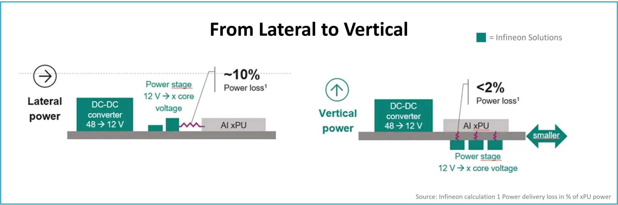
Fig 2. From Lateral to Vertical
Compared to traditional Side-by-Side layouts, the implementation of the vertical power delivery architecture achieves the following breakthroughs (data based on ASE test results):
- Drastically Reduced Transmission Loss: By significantly shortening the current transmission path, Transmission Loss drops from the traditional 12% to approximately 6%, representing a reduction of over 50%.
- Significantly Increased Power Density: Through 3D stacking and embedded technologies, power density improves from 0.4 A/mm² to 0.6 A/mm², increasing power delivery capacity per unit area by 50%.
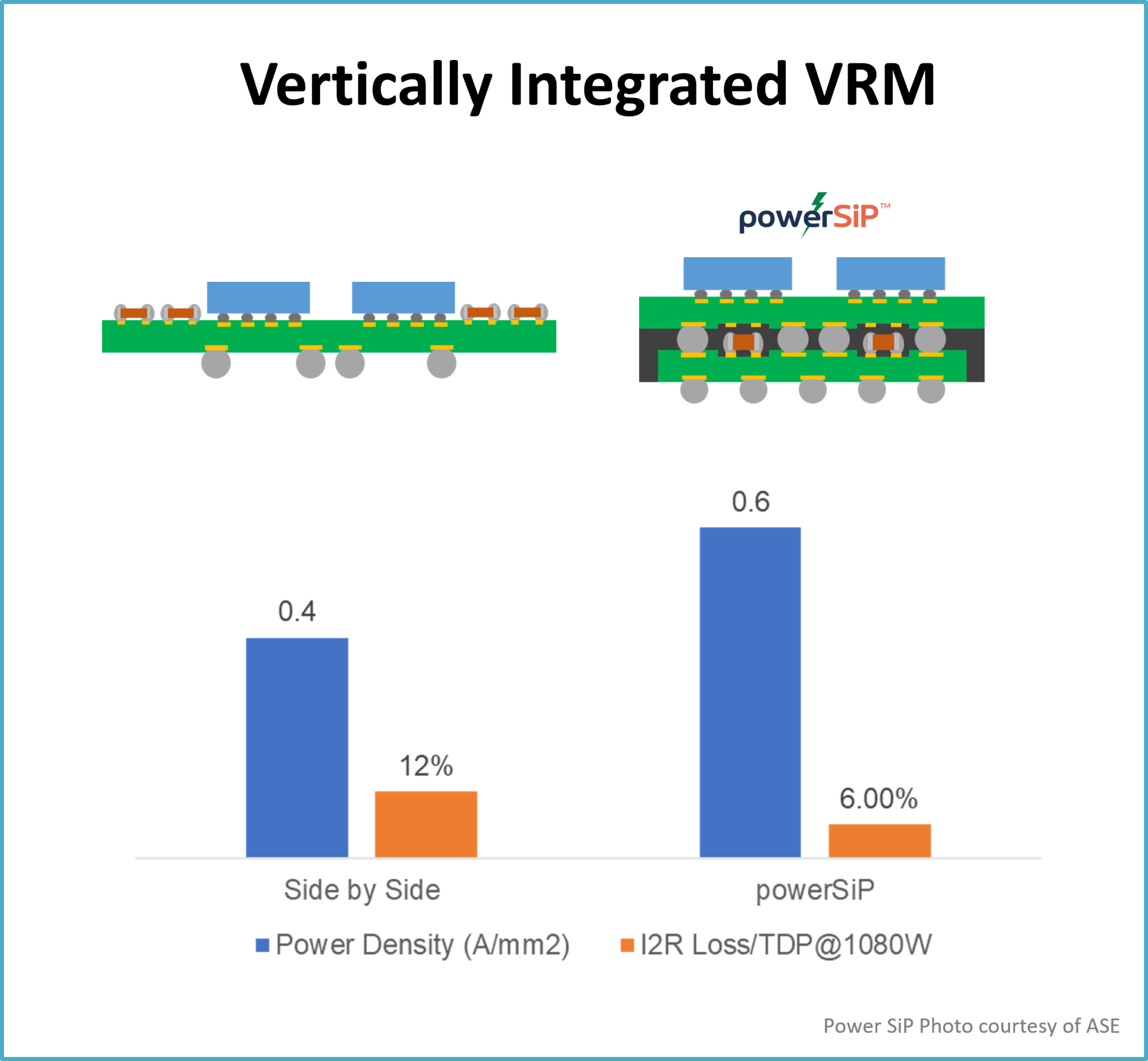
Fig. 3 Vertically Integrated VRM
Core Technology Analysis: Power Block Modulization Technology
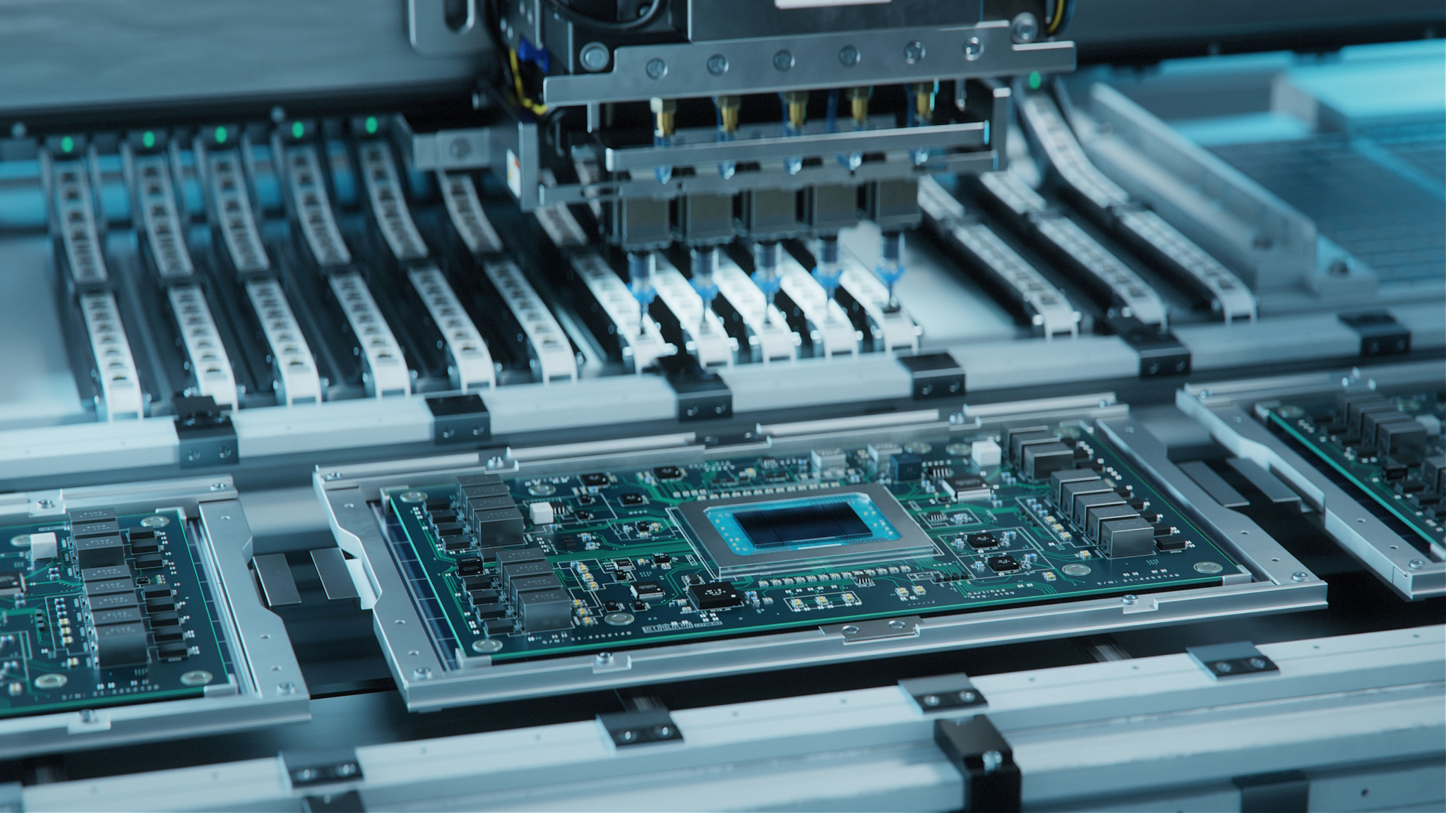
At the technical implementation level, USI’s strategic core lies in the structural optimization and manufacturing innovation of the Power Block. We go beyond assembly, diving deep into the internal structural design of components to integrate the inductor, capacitor, MOSFET, and driver into a single high-density module.
Learn More: Event |【Wide-Bandgap Semiconductor Technology Forum】: How Modularization and Miniaturization Revolutionize Server Power Efficiency
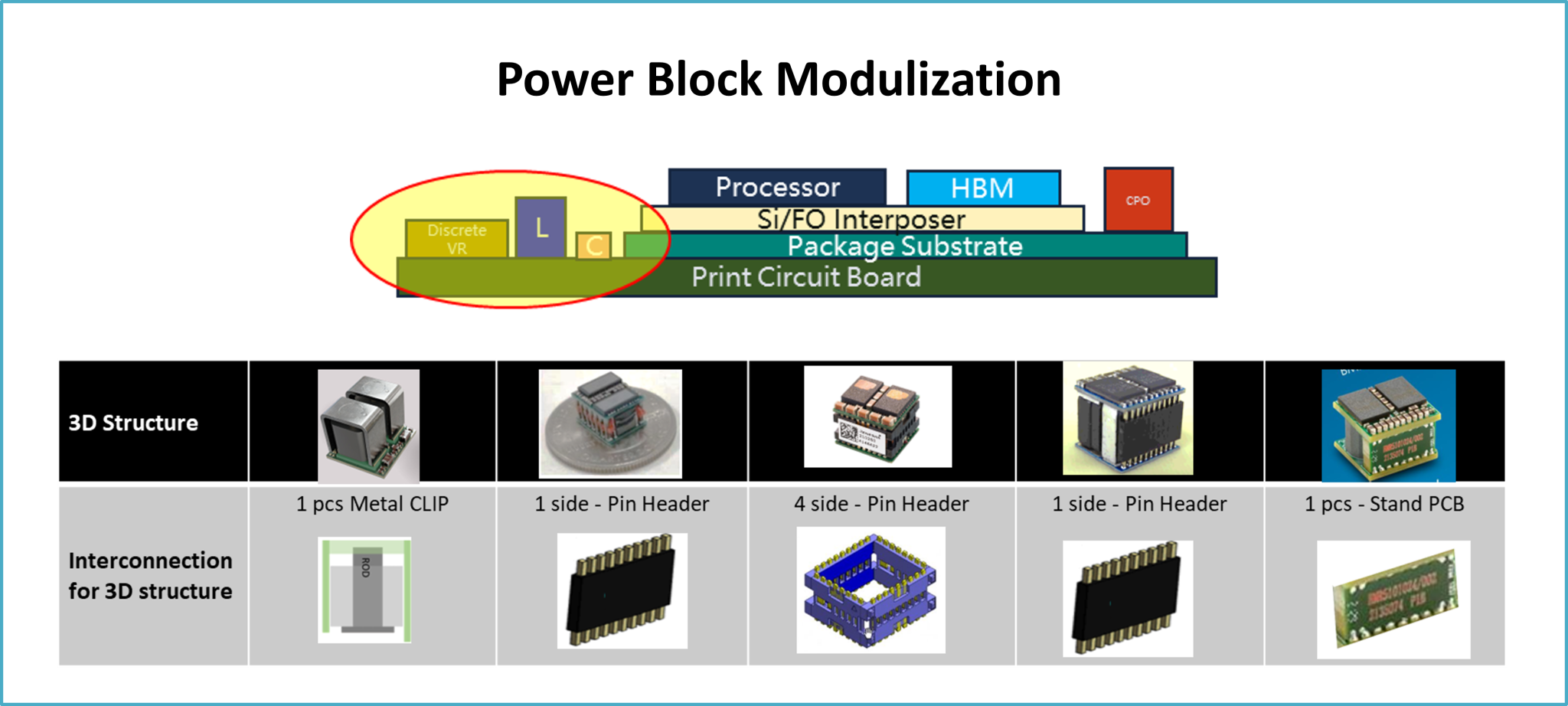
Fig 4. Power Block Modulization
Challenges and Practices in Miniaturization: To accommodate denser server configurations, module thickness must be continuously compressed. From 8mm in the past to 5mm, USI is currently challenging the limit of 4mm.
- 3D Structure Optimization: We utilize Metal Clips and Pin Headers to establish vertical interconnections, replacing space-consuming traditional wiring .
- Thermal & Grounding Management: Addressing the grounding and thermal requirements of PMIC QFN packages, we employ chip-embedded or low void bonding technology to ensure thermal stability under high-current operation.
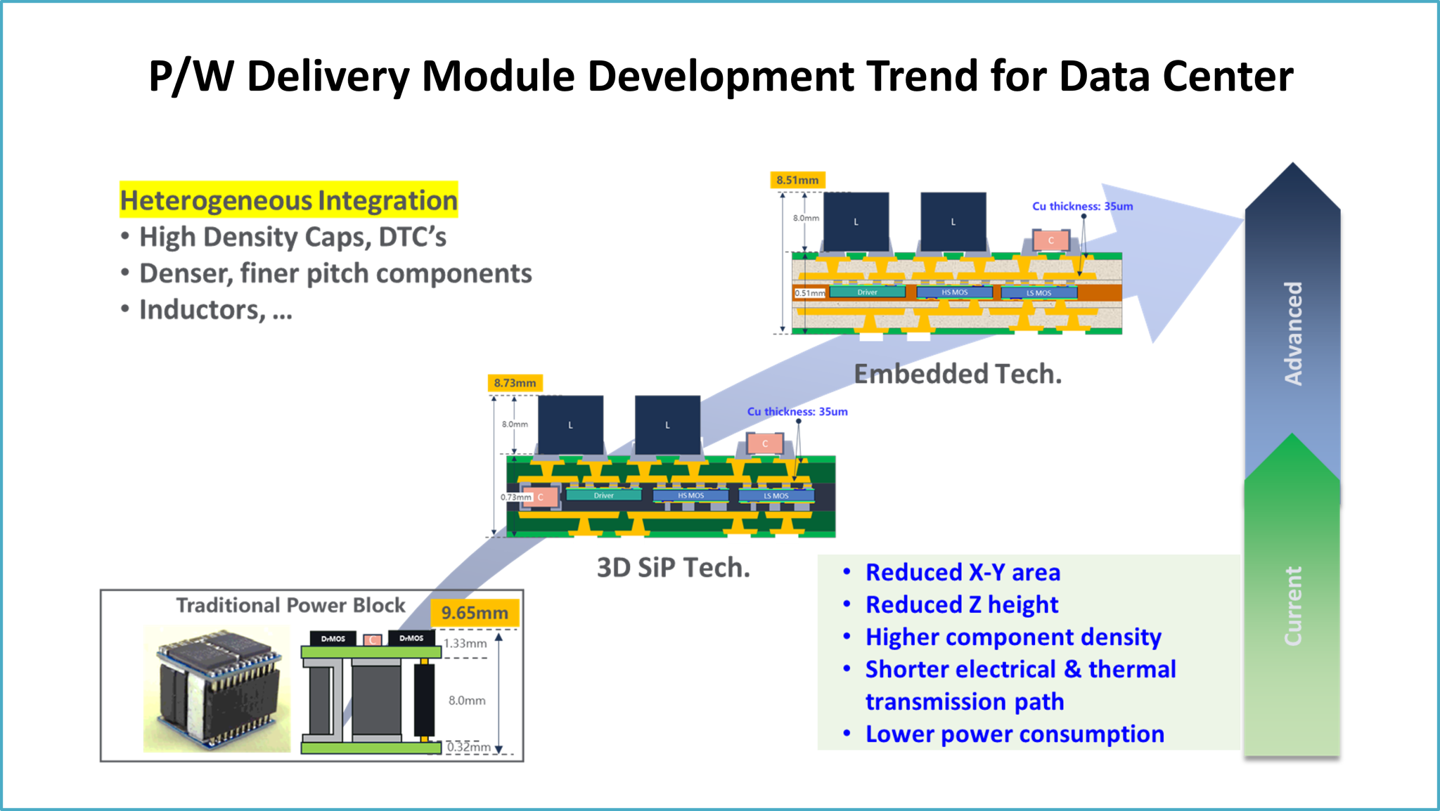
Fig 5. P/W Delivery Module Development Trend for Data Center_Source: ASE Holdings
Future Trend Forecast: 800V HVDC and IVR Integration
1. Shifting to 800V High Voltage DC (HVDC)
For the future architecture of data centers, USI and ASE Holdings are working together to develop the next phase of our technology road-map. As single-rack power consumption moves from 100kW toward 1MW, traditional 48V distribution architectures face immense challenges. We are actively developing power modules that support 800V DC.
- Physics Principle: According to P = IV and Ploss = I2R, increasing voltage significantly reduces current, thereby drastically cutting thermal loss during transmission.
- Weight Reduction Advantage: Lower current allows the use of thinner copper cables, solving the structural issue of excessive weight in current AI server racks caused by massive, thick copper cabling .
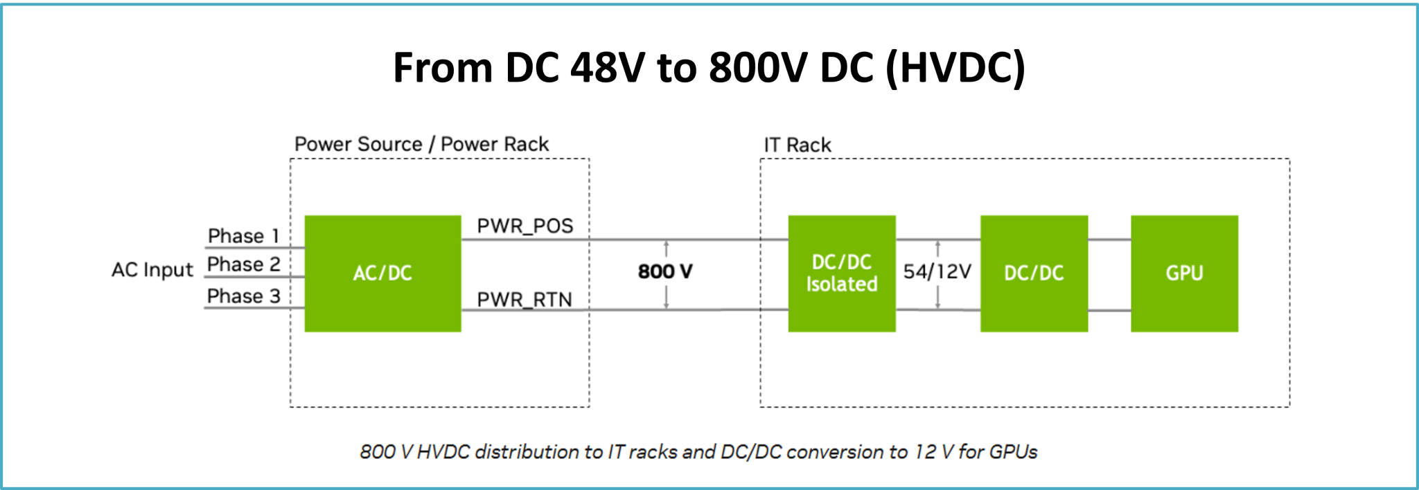
Fig 6. From DC 48V to 800V DC
2. Integrated Voltage Regulator (IVR)
Looking further into the future, power delivery will be further integrated into the silicon interposer (CoWoS) within the chip. As a leader in modularization technology, USI acts as the critical bridge connecting "board-level power" and "chip-level power (IVR)," offering a complete conversion solution from 48V down to 1V .
Breaking the Energy Efficiency Wall with USI
Dr. Shen’s presentation effectively positioned USI (Universal Scientific Industrial / Ring Universal Electronics) not merely as an assembler, but as a co-developer of critical AI infrastructure. We, USI, possess the industry's most comprehensive "Toolbox," covering end-to-end capabilities from chip packaging and module design to system assembly, including a number of key technical advantages:
- End-to-End Integration Capability: Unlike competitors who focus on single stages, USI spans the entire value chain: from system packaging and module design to system integration. This allows USI to optimize power delivery holistically, solving problems at the module level that resolve constraints at the system level.
- Leadership in Miniaturization (3D SiP): USI has proven expertise in embedded passives, and advanced molding.
- Thermal & Signal Integrity Expertise: By mastering the "power block," USI is better able to provide solutions to the dual challenges of removing heat from increasingly dense clusters and ensuring clean power delivery to sensitive processors.
Search
Recent Articles
-
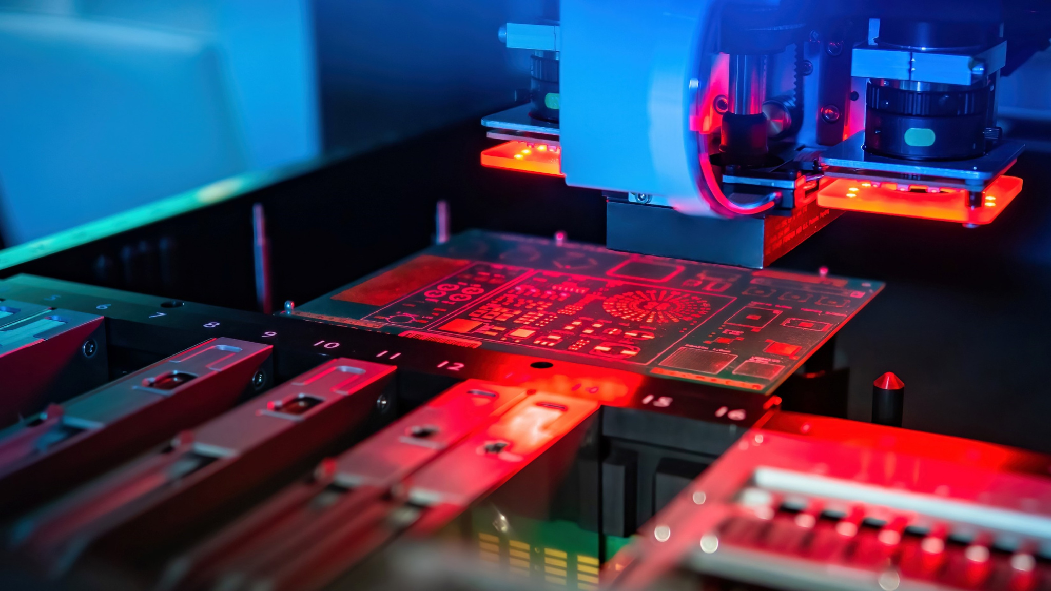
When AI Learns to “Read”: Using Deep Learning to Tame the False-Alarm Storm on SMT Production Lines
 When AI Learns to “Read”: Using Deep Learning to Tame the False-Alarm Storm on SMT Production Lines
07/13/2026
When AI Learns to “Read”: Using Deep Learning to Tame the False-Alarm Storm on SMT Production Lines
07/13/2026
-
Catching Invisible “Micro-Failures”: Safeguarding SiP Reliability Testing with Daisy Chains
 Catching Invisible “Micro-Failures”: Safeguarding SiP Reliability Testing with Daisy Chains
06/29/2026
Catching Invisible “Micro-Failures”: Safeguarding SiP Reliability Testing with Daisy Chains
06/29/2026
-
The Hidden Rival Inside an EV’s Heart: Cracking the Power-Loss Puzzle with “Physical Modeling”
 The Hidden Rival Inside an EV’s Heart: Cracking the Power-Loss Puzzle with “Physical Modeling”
06/17/2026
The Hidden Rival Inside an EV’s Heart: Cracking the Power-Loss Puzzle with “Physical Modeling”
06/17/2026
-
Behind the MFG. | From "Manufacturing" to "Creation" Ep.2: Innovation Built from Zero to One
 Behind the MFG. | From "Manufacturing" to "Creation" Ep.2: Innovation Built from Zero to One
05/28/2026
Behind the MFG. | From "Manufacturing" to "Creation" Ep.2: Innovation Built from Zero to One
05/28/2026
-
Behind the MFG. | From "Manufacturing" to "Creation" Ep.1: Unveiling USI’s Technological Vanguard
 Behind the MFG. | From "Manufacturing" to "Creation" Ep.1: Unveiling USI’s Technological Vanguard
05/07/2026
Behind the MFG. | From "Manufacturing" to "Creation" Ep.1: Unveiling USI’s Technological Vanguard
05/07/2026
-
Breaking the AI Energy Wall: Power Block and 3D Miniaturization Solutions
 Breaking the AI Energy Wall: Power Block and 3D Miniaturization Solutions
12/31/2025
Breaking the AI Energy Wall: Power Block and 3D Miniaturization Solutions
12/31/2025
-
Mastering Automotive HPC: Defining the "Sweet Spot" of SoMoG Technology
 Mastering Automotive HPC: Defining the "Sweet Spot" of SoMoG Technology
12/15/2025
Mastering Automotive HPC: Defining the "Sweet Spot" of SoMoG Technology
12/15/2025
-
【Smart Power Supply】Innovative Solution for DAC Control Bias Current
 【Smart Power Supply】Innovative Solution for DAC Control Bias Current
10/21/2025
【Smart Power Supply】Innovative Solution for DAC Control Bias Current
10/21/2025
-
From Experience to Precision: How AI Algorithms Enable Efficient RF Prediction Models
 From Experience to Precision: How AI Algorithms Enable Efficient RF Prediction Models
09/11/2025
From Experience to Precision: How AI Algorithms Enable Efficient RF Prediction Models
09/11/2025
-
Event|DIGITIMES 2025 D Forum – USI Shares How Heterogeneous Integration Drives a New Landscape for MCU Applications
 Event|DIGITIMES 2025 D Forum – USI Shares How Heterogeneous Integration Drives a New Landscape for MCU Applications
08/15/2025
Event|DIGITIMES 2025 D Forum – USI Shares How Heterogeneous Integration Drives a New Landscape for MCU Applications
08/15/2025
Keep up with top trending topic
For the latest innovation technology, application
and industry insight.
Subscribe Our Blog
For the latest innovation technology, application
and industry insight.