USI Blog
Top trending topic for the latest innovation technology, application and industry insight.
Search
- 06/20/2025
Event |【Wide-Bandgap Semiconductor Technology Forum】: How Modularization and Miniaturization Revolutionize Server Power Efficiency
Speaker: John Fang, Ph.D., CTO and Corp. SVP of USI
On June 12th, at the invitation of our industry media partner " Micro-electronics", John, our Chief Technology Officer, was honored to be one of the keynote speakers of the "Wide-Bandgap Semiconductor Technology Trends and Industrial Applications Summit Forum" to share the technology development in the field of AI, especially the topic of power supply, with the industry leaders. When we talk about high-performance computing (HPC) and AI, the idea is often faster processors, larger high-bandwidth memory (HBM), and advanced packaging technologies such as 3D IC stacks and fan-out wafer-level packaging. However, behind this arms race of computing power, a more fundamental challenge is becoming more and more severe, that is, "power supply".
It is no exaggeration to say that AI has been described as an "electricity-eating monster", and we urgently need more innovative ways to improve energy efficiency. USI's power module business plays a pivotal role in two high-growth segments: electric vehicles (EVs) and AI servers. Today, we're going to dive into this key topic: “Power Supply”, with a focus on the power efficiency challenges and solutions of AI servers. In this keynote, John focused on sharing how USI can build a more efficient and energy-saving power heart for AI servers through modulization and miniaturization.
Energy Alarm Bells in the Age of AI
First, John specifically pointed out that we must face up to the seriousness of the problem. The power consumption of GPUs is skyrocketing at an alarming rate. In the case of NVIDIA's products, from A100 to H100, power consumption has increased by 75% in just one generation. The latest B200 consumes up to 1,200W, and the future R200 is expected to reach 1,800W. AMD's and Intel's product lines are showing a similar trend, with power consumption increasing by 50%.
It's not just numbers on a single chip. Elon Musk, the founder of xAI, has mentioned that his Grok 2 model requires 20,000 NVIDIA H100 GPUs, while the Grok 3 requires up to 100,000 GPUs. This means that the GPU alone requires about 100MW of power, and if you add servers and cooling systems, its "supercomputing cluster" in Memphis has even applied for 150MW of electricity from the local power company, enough to supply tens of thousands of homes.
In a typical data center, power conversion alone accounts for 11% of total energy consumption. When we are faced with total power consumption in the megawatt range, any increase in efficiency is crucial.
The Limits of the Traditional “Side-by-Side”
Traditionally, engineers have optimized at the chip level to improve power efficiency. For example:
- Using a lower power stage can improve efficiency by about 1.6%.
- Choke, which has a lower inductance of DC resistance (DCR), can be improved by approximately 0.2%.
- Adjust the switching frequency of the voltage regulator (VR) by about 0.2%.
The Revolution from Horizontal Side-by-Side to Vertical Integration
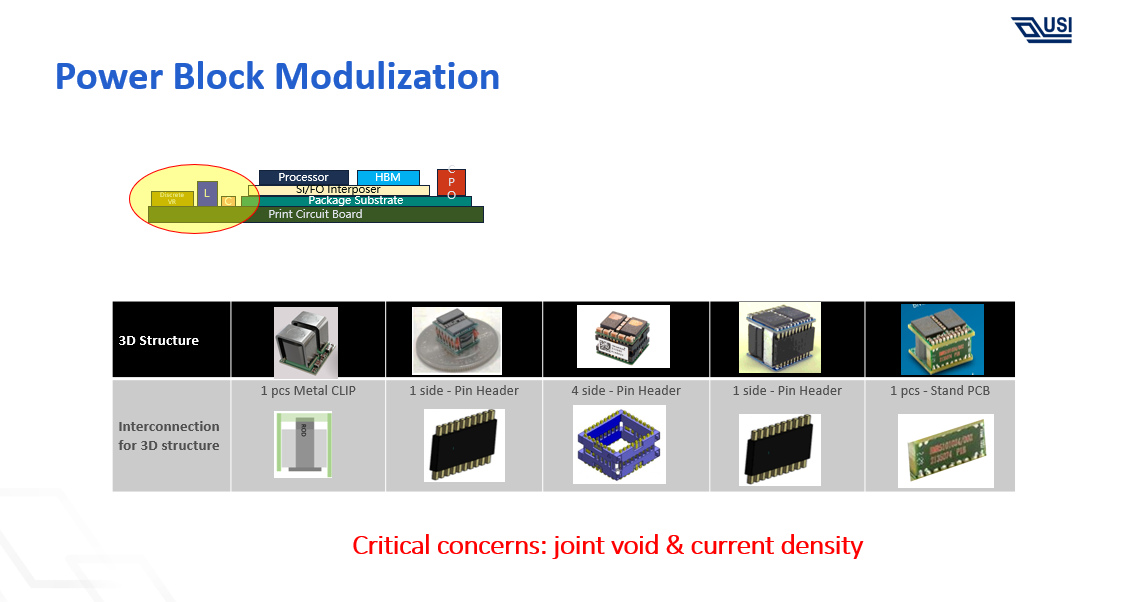
Step 1: Stacked Power Modules (Modularization) The solution is to pre-integrate discrete components such as DrMOS, inductors, and capacitors into a 3D stacked power module (Power Block). This modular design not only saves PCB space but also paves the way for standardized production. There are already various solutions on the market, but process challenges such as joint voids and current density still need to be overcome.
Step 2: Vertically Integrated VRM (Miniaturization) This is the real revolution. Instead of placing power modules side-by-side next to the processor, we vertically integrate them below the processor package, bringing the power infinitely close to the point-of-load.
This "Vertically Integrated VRM" brings amazing benefits:
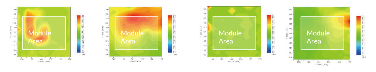
- Size and Path Reduction: The VRM is directly located below the SoC, making the power transmission path extremely short, significantly reducing copper loss (I2R Loss). Compared to traditional side-by-side designs, the footprint is reduced by 25%.
- Efficiency Improvement: In a 1080W TDP test, the routing power loss of the side-by-side design was as high as 12%, while the vertically integrated powerSIP solution dropped sharply to 6%, halving the loss.
- Power Density Doubling: The current density increased from 0.4 A/mm² in the side-by-side design to 0.6 A/mm² in the vertical design.
Integrated Voltage Regulator (IVR) in the Chip
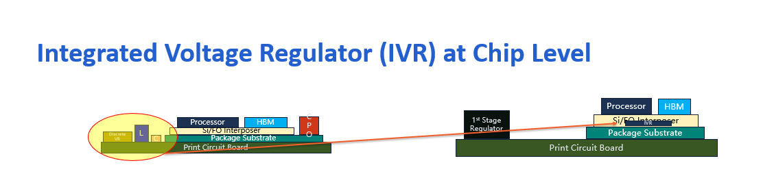
Looking ahead, the ultimate form of power technology is the Integrated Voltage Regulator (IVR). This is a technology that integrates high-efficiency switching regulators and passive components directly into a single chip, with advantages including:
- Zero Discrete Components: Extremely small size, can be directly installed inside the SoC substrate, even under the BGA, with a thickness as thin as 100um.
- Ultra-Fast Response: With dynamic voltage regulation (DVS) capability 1000 times faster than traditional designs, it can respond to load changes within nanoseconds, providing the most precise voltage and eliminating unnecessary power waste.
- Elimination of Losses and External Components: Due to its proximity to the load, it almost eliminates I²R losses and no longer requires a large number of external decoupling capacitors, further reducing system cost and complexity.
From System to Package, Creating a High-Performance Green Engine for Future AI
The current energy supply trend is quite clear. Tesla has directly placed power components under the GPU in its AI hardware. AMD and Microsoft have also introduced similar specifications in their next-generation AI servers, and some manufacturers are even developing IVR technology that integrates VRM directly into the processor silicon.
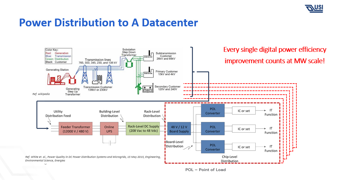
The entire power conversion path is constantly evolving, from cabinet-level 48V input, stepping down to 12V on the motherboard or directly 48V power supply, and finally down to the core voltage required by the chip. Miniaturization and efficiency improvement are the main focus of our technology development at every link in this chain.
Finally, John concluded that to cope with the computing power and power consumption challenges of the AI era, power design is moving from traditional side-by-side to revolutionary vertical integration. This is not just a rearrangement of components, but a comprehensive optimization of space, path, and efficiency through structural innovation. The core spirit of this path is to simplify design complexity through modularization and shorten physical distance and reduce energy loss through miniaturization. Only in this way can we create an ultimate heart with both powerful performance and green energy-saving for the computing-driven future.
Search
Recent Articles
-
When AI Learns to “Read”: Using Deep Learning to Tame the False-Alarm Storm on SMT Production Lines
 When AI Learns to “Read”: Using Deep Learning to Tame the False-Alarm Storm on SMT Production Lines
07/13/2026
When AI Learns to “Read”: Using Deep Learning to Tame the False-Alarm Storm on SMT Production Lines
07/13/2026
-
Catching Invisible “Micro-Failures”: Safeguarding SiP Reliability Testing with Daisy Chains
 Catching Invisible “Micro-Failures”: Safeguarding SiP Reliability Testing with Daisy Chains
06/29/2026
Catching Invisible “Micro-Failures”: Safeguarding SiP Reliability Testing with Daisy Chains
06/29/2026
-
The Hidden Rival Inside an EV’s Heart: Cracking the Power-Loss Puzzle with “Physical Modeling”
 The Hidden Rival Inside an EV’s Heart: Cracking the Power-Loss Puzzle with “Physical Modeling”
06/17/2026
The Hidden Rival Inside an EV’s Heart: Cracking the Power-Loss Puzzle with “Physical Modeling”
06/17/2026
-
Behind the MFG. | From "Manufacturing" to "Creation" Ep.2: Innovation Built from Zero to One
 Behind the MFG. | From "Manufacturing" to "Creation" Ep.2: Innovation Built from Zero to One
05/28/2026
Behind the MFG. | From "Manufacturing" to "Creation" Ep.2: Innovation Built from Zero to One
05/28/2026
-
Behind the MFG. | From "Manufacturing" to "Creation" Ep.1: Unveiling USI’s Technological Vanguard
 Behind the MFG. | From "Manufacturing" to "Creation" Ep.1: Unveiling USI’s Technological Vanguard
05/07/2026
Behind the MFG. | From "Manufacturing" to "Creation" Ep.1: Unveiling USI’s Technological Vanguard
05/07/2026
-
Breaking the AI Energy Wall: Power Block and 3D Miniaturization Solutions
 Breaking the AI Energy Wall: Power Block and 3D Miniaturization Solutions
12/31/2025
Breaking the AI Energy Wall: Power Block and 3D Miniaturization Solutions
12/31/2025
-
Mastering Automotive HPC: Defining the "Sweet Spot" of SoMoG Technology
 Mastering Automotive HPC: Defining the "Sweet Spot" of SoMoG Technology
12/15/2025
Mastering Automotive HPC: Defining the "Sweet Spot" of SoMoG Technology
12/15/2025
-
【Smart Power Supply】Innovative Solution for DAC Control Bias Current
 【Smart Power Supply】Innovative Solution for DAC Control Bias Current
10/21/2025
【Smart Power Supply】Innovative Solution for DAC Control Bias Current
10/21/2025
-
From Experience to Precision: How AI Algorithms Enable Efficient RF Prediction Models
 From Experience to Precision: How AI Algorithms Enable Efficient RF Prediction Models
09/11/2025
From Experience to Precision: How AI Algorithms Enable Efficient RF Prediction Models
09/11/2025
-
Event|DIGITIMES 2025 D Forum – USI Shares How Heterogeneous Integration Drives a New Landscape for MCU Applications
 Event|DIGITIMES 2025 D Forum – USI Shares How Heterogeneous Integration Drives a New Landscape for MCU Applications
08/15/2025
Event|DIGITIMES 2025 D Forum – USI Shares How Heterogeneous Integration Drives a New Landscape for MCU Applications
08/15/2025
Keep up with top trending topic
For the latest innovation technology, application
and industry insight.
Subscribe Our Blog
For the latest innovation technology, application
and industry insight.