USI Blog
Search
- 06/09/2025
FEDS: A Key Engine Driving RF Automation Development

Wireless communication capabilities have become an indispensable part of modern electronic products. From smartphones to IoT devices, the demand for wireless functionality is growing increasingly complex and diverse. This trend presents unprecedented challenges to the Radio Frequency (RF) design teams within the electronics manufacturing industry. Building upon the automation benefits of USI's FEDS platform, previously demonstrated in circuit layout review and power integrity simulation, this article is continuing to delve into FEDS's automated applications in the RF design domain and how it helps engineers overcome complexity and boost efficiency.
Three Major Challenges in RF Design: Complexity, Efficiency, and Talent Gap
Integrating multiple wireless communication standards (such as Wi-Fi, Bluetooth, cellular networks, etc.) into a single product is now standard practice, significantly increasing the complexity of RF circuitry. For RF simulation engineers, a primary and time-consuming task in the traditional workflow is identifying and extracting all RF paths from complex schematics. A single project might involve hundreds of RF paths, encompassing antenna sharing, band sharing, and co-location circuitry. In the past, due to tight development schedules, engineers were often forced to manually select and simulate only a subset of key paths, which undoubtedly increased design risks.
Manual RF simulation setup represents another significant efficiency bottleneck. Each RF path requires a tedious multi-step setup process within simulation tools. Data suggests this could involve over 19 steps to run a simulation successfully. This highly repetitive and time-consuming work not only consumes valuable engineering time but also limits a company's capacity to undertake more complex high-frequency projects. Furthermore, RF simulation demands highly specialized knowledge and experience. Qualified simulation engineers are relatively scarce in the job market, exacerbating human resource pressures.
Automation from Simulation to Measurement: Integrated Workflow Application
To address the pain points mentioned above, USI's CE R&D team developed the "RF Automation Development Function" on the FEDS platform (FEDS-RF). The core advantage of this system lies in automating key processes within RF design, thereby significantly improving efficiency and lowering the technical barrier to entry. Traditional RF design, from matching and simulation to actual measurement, often involves cross-functional teamwork with high communication overhead. The RF automation development function, through its cloud architecture integrated with internal servers, achieves a automated simulation and testing workflow:
- Automatic upload of Layout/BOM data
- The system automatically performs matching and simulation based on RF requirements
- Generates result reports after simulation and automatically compares them with measurement data
- Automatically flags abnormal items and provides correction suggestions
- All records are stored in the system for future review and optimization
- Engineers only need to review results and make strategic adjustments, substantially reducing operational burden.
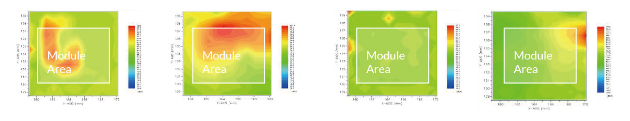
Case Study: RF Dev. Function Application in Multi-band Wi-Fi Module Design
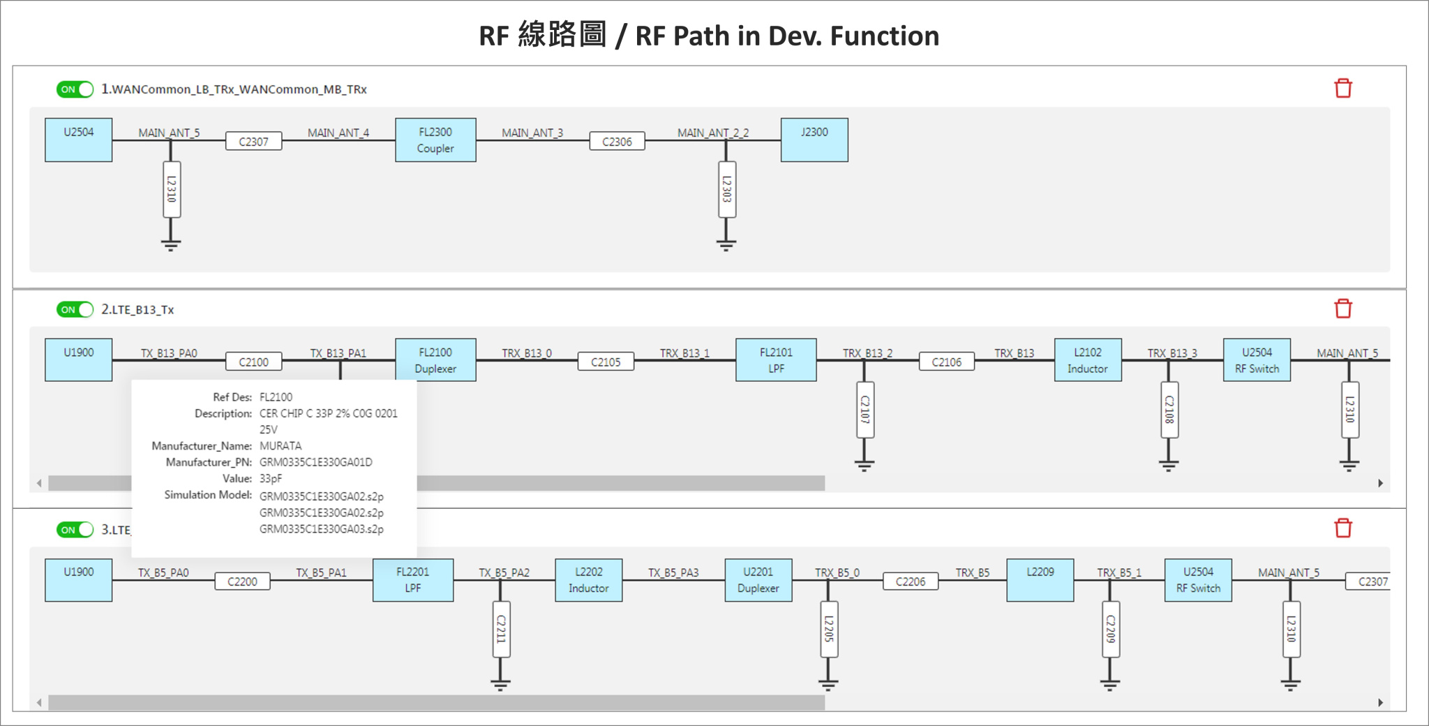
Fig1. The RF route map was retrieved from the complex schematic and be redrawn separately
Taking a communication module supporting both 2.4GHz and 5GHz Wi-Fi as an example, traditional design requires individual matching and testing for each frequency band. This is a lengthy process, typically it took 2 weeks to complete the test job for a development project with 2 engineers, but after implementing the RF automation development function, it can be completed in 3 days.
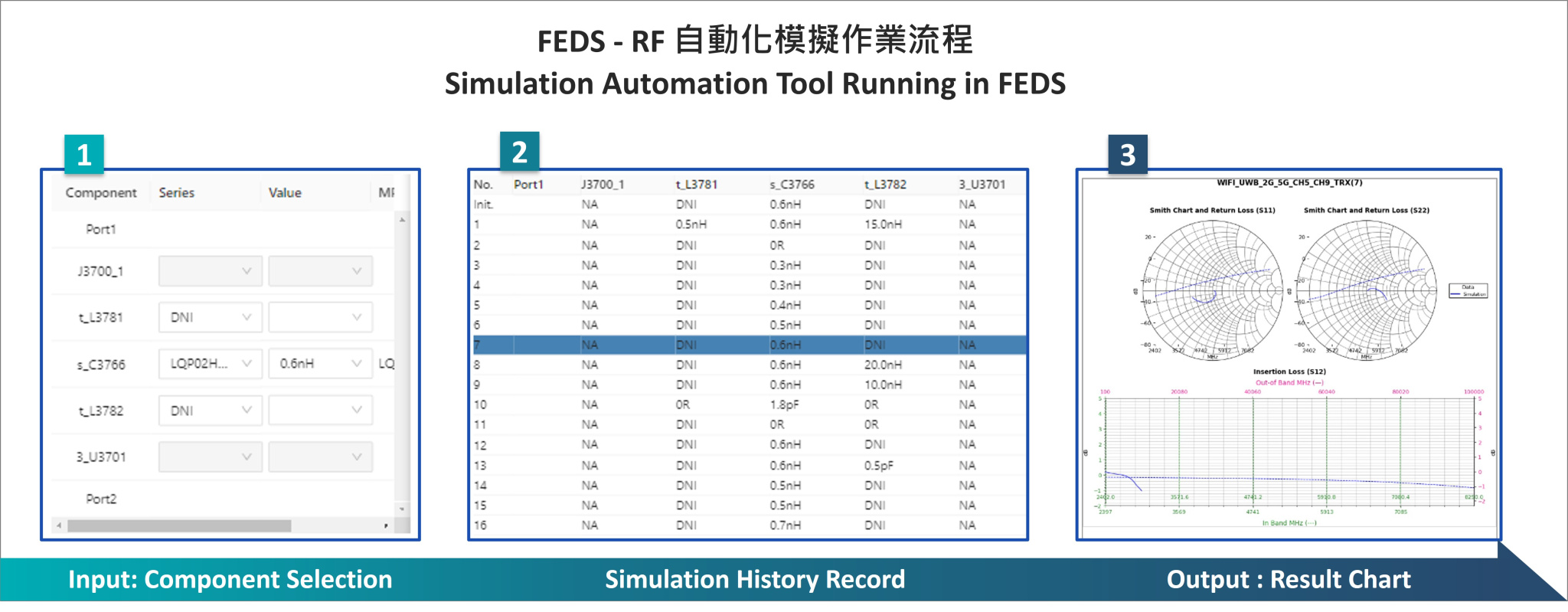
Fig2. Interface for matching simulation, including part selection, simulation history records, and results
- Automatic completion of matching circuit design and simulation.
- The system performs real-time analysis based on target S11/S21 specifications.
- Test reports are generated within 1 hour after simulation completion.
- This not only saves significant human resources but also improves the RF performance consistency of the final product.
As can be seen from the above practical applications, the RF automation development function has demonstrated impressive efficiency. Industry field tests show that RF path checking time can be drastically reduced from a traditional 100 hours to approximately 12 hours. Previously, simulation engineers could manually create simulation environments for a maximum of 80 paths. Now, the automation development function can automatically process over 130 paths, significantly enhancing coverage and accuracy. The development team is already moving towards the next milestone, starting from a human mindset and finding the best solution for the project requirements through this automated development tool. Compared to traditional approaches, automated development tools bring significant benefits at different levels of the overall project.
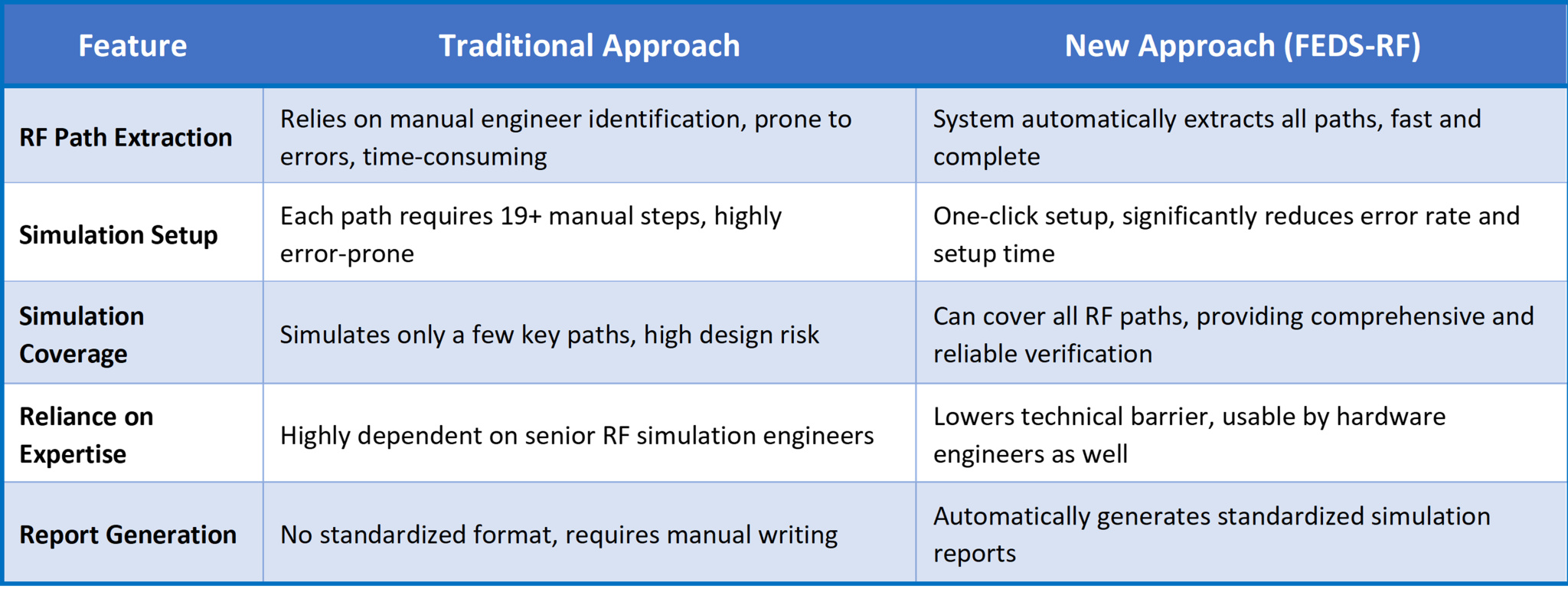
Table1. Benefits at different levels brought by RF Dev. Function
Consistency, High Efficiency, Data-Driven Design Process
According to internal implementation data from USI, the RF automation development function has yielded the following key results:
- Design Consistency Improved: Matching and verification are performed using fixed algorithms, reducing design result variations among different engineers.
- Time Savings Up to 70%: Automated matching and simulation replace manual work, saving, on average, over half of the development effort.
- Error Rate Reduced by 90%: The platform includes built-in critical design parameter constraints, reducing manual setup errors.
- Transparent Knowledge Transfer: Through historical data storage and comparison, the high dependency on senior engineers is reduced.
From circuit layout and power integrity simulation to the comprehensive automation of RF design, USI is not merely developing a set of tools but systematically transforming years of accumulated project experience and engineering knowledge into a scalable automated platform. This mindset of "Experience Digitization, Process Modularization, Performance Benchmarking" is a microcosm of the development trend in RF design automation. Through the development function, we demonstrate our capability to integrate cross-disciplinary expertise and strengthen our core corporate competencies. Simultaneously, using this platform's cloud architecture as a leverage point, we have built a foundation of flexibility and scalability to face future design challenges involving increased device co-existence, multi-band, and multi-module integration. This undoubtedly enables us to respond to market demands more agilely.
FAQs for FEDS-RF Project
Q1: What is the FEDS platform?
A1: The FEDS platform is a radio frequency (RF) design automation development system developed by USI Electronics, aimed at improving RF design efficiency and lowering technical barriers.
Q2: What are the main challenges faced in RF design?
A2: RF design faces three main challenges: complexity, efficiency, and talent shortage. Integrating multiple wireless communication standards increases circuit complexity, manual simulation settings are cumbersome and time-consuming, and it requires highly specialized knowledge and experience.
Q3: How does the FEDS platform address the challenges of RF design?
A3: The FEDS platform automates matching and simulation, reducing manual operations, improving efficiency, and lowering reliance on specialized talent. It achieves automation of simulation and measurement, reducing inter-departmental communication costs.
Q4: What is the core advantage of the RF automation development function?
A4: The core advantage of the RF automation development function is automating key processes in RF design, significantly improving efficiency and lowering technical barriers.
Q5: What is the application effect of the RF automation development function in practice?
A5: In multi-band Wi-Fi module design, the RF automation development function reduces testing time from 2 weeks to within 3 days, significantly improving development efficiency.
Q6: What are the comprehensive benefits brought by the RF automation development function?
A6: The RF automation development function reduces RF path inspection time from 100 hours to about 12 hours and can automatically handle over 130 paths, improving accuracy and coverage.
Search
Recent Articles
-
When AI Learns to “Read”: Using Deep Learning to Tame the False-Alarm Storm on SMT Production Lines
 When AI Learns to “Read”: Using Deep Learning to Tame the False-Alarm Storm on SMT Production Lines
07/13/2026
When AI Learns to “Read”: Using Deep Learning to Tame the False-Alarm Storm on SMT Production Lines
07/13/2026
-
Catching Invisible “Micro-Failures”: Safeguarding SiP Reliability Testing with Daisy Chains
 Catching Invisible “Micro-Failures”: Safeguarding SiP Reliability Testing with Daisy Chains
06/29/2026
Catching Invisible “Micro-Failures”: Safeguarding SiP Reliability Testing with Daisy Chains
06/29/2026
-
The Hidden Rival Inside an EV’s Heart: Cracking the Power-Loss Puzzle with “Physical Modeling”
 The Hidden Rival Inside an EV’s Heart: Cracking the Power-Loss Puzzle with “Physical Modeling”
06/17/2026
The Hidden Rival Inside an EV’s Heart: Cracking the Power-Loss Puzzle with “Physical Modeling”
06/17/2026
-
Behind the MFG. | From "Manufacturing" to "Creation" Ep.2: Innovation Built from Zero to One
 Behind the MFG. | From "Manufacturing" to "Creation" Ep.2: Innovation Built from Zero to One
05/28/2026
Behind the MFG. | From "Manufacturing" to "Creation" Ep.2: Innovation Built from Zero to One
05/28/2026
-
Behind the MFG. | From "Manufacturing" to "Creation" Ep.1: Unveiling USI’s Technological Vanguard
 Behind the MFG. | From "Manufacturing" to "Creation" Ep.1: Unveiling USI’s Technological Vanguard
05/07/2026
Behind the MFG. | From "Manufacturing" to "Creation" Ep.1: Unveiling USI’s Technological Vanguard
05/07/2026
-
Breaking the AI Energy Wall: Power Block and 3D Miniaturization Solutions
 Breaking the AI Energy Wall: Power Block and 3D Miniaturization Solutions
12/31/2025
Breaking the AI Energy Wall: Power Block and 3D Miniaturization Solutions
12/31/2025
-
Mastering Automotive HPC: Defining the "Sweet Spot" of SoMoG Technology
 Mastering Automotive HPC: Defining the "Sweet Spot" of SoMoG Technology
12/15/2025
Mastering Automotive HPC: Defining the "Sweet Spot" of SoMoG Technology
12/15/2025
-
【Smart Power Supply】Innovative Solution for DAC Control Bias Current
 【Smart Power Supply】Innovative Solution for DAC Control Bias Current
10/21/2025
【Smart Power Supply】Innovative Solution for DAC Control Bias Current
10/21/2025
-
From Experience to Precision: How AI Algorithms Enable Efficient RF Prediction Models
 From Experience to Precision: How AI Algorithms Enable Efficient RF Prediction Models
09/11/2025
From Experience to Precision: How AI Algorithms Enable Efficient RF Prediction Models
09/11/2025
-
Event|DIGITIMES 2025 D Forum – USI Shares How Heterogeneous Integration Drives a New Landscape for MCU Applications
 Event|DIGITIMES 2025 D Forum – USI Shares How Heterogeneous Integration Drives a New Landscape for MCU Applications
08/15/2025
Event|DIGITIMES 2025 D Forum – USI Shares How Heterogeneous Integration Drives a New Landscape for MCU Applications
08/15/2025
For the latest innovation technology, application
and industry insight.