USI Blog
Top trending topic for the latest innovation technology, application and industry insight.
Search
- 05/23/2023
Harnessing the Power of PCIe 5.0 and PCB Simulation for Next-Gen Technologies
The digital world has been witnessed significant technological advancements in the past few years, especially in terms of the data transmission and processing speeds. Technologies such as AI (Artificial Intelligence), IoT (Internet of Things) and 5G are becoming increasingly mature and widely used, with PCI Express (PCIe) technology playing an important role in these industries. The emergence of PCIe 5.0 has created a buzz in the tech industry as it promises to bring significant improvements in terms of performance and speed. Along with the latest PCB simulation technologies, PCIe 5.0 can revolutionize how we perceive and use technology.
What is PCIe?
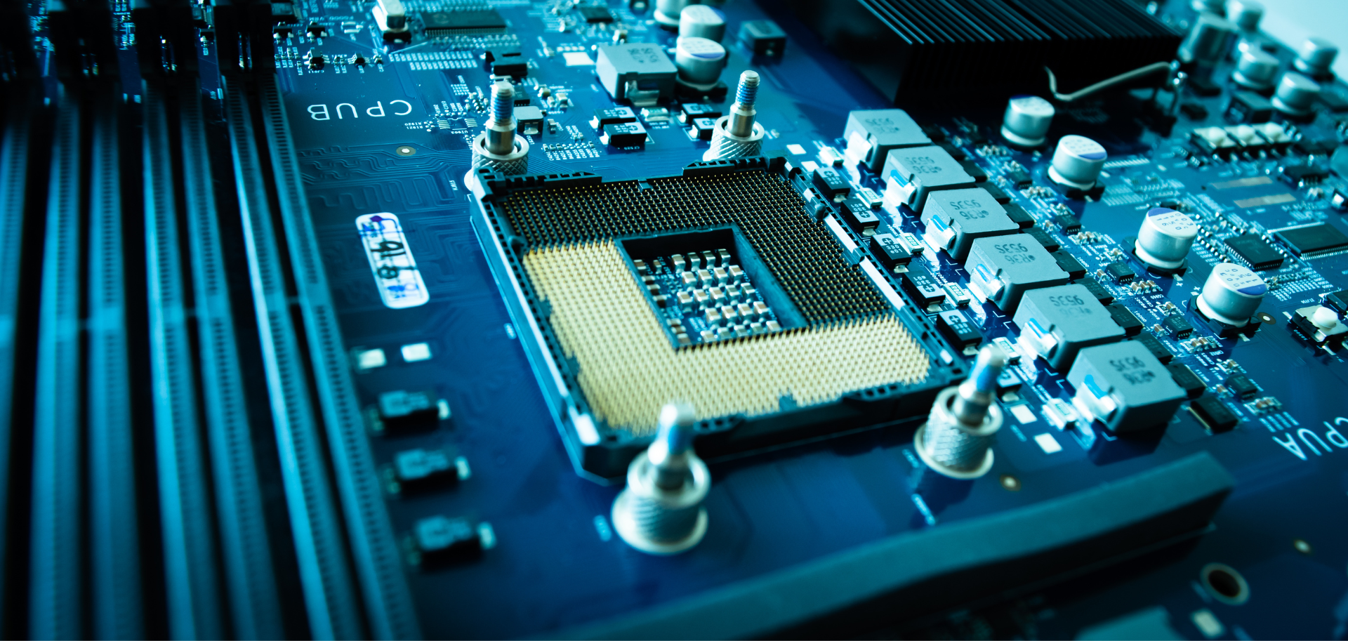
PCIe is a high-speed serial computer expansion bus standard that serves as the primary backbone for data transfer between different components of a computer system, such as the CPU and GPU or other accelerated processors. The PCIe 5.0, for example, is currently being developed at 32 GT/s, twice the speed of PCIe 4.0. With the ability to transfer 128GB/s (gigabits per second) in a 16-lane configuration, PCIe 5.0 not only provides a high-speed, reliable data transfer channel but also has the flexibility to scale to meet the demands of processing large amounts of data, including artificial intelligence, machine learning and data analysis.
Learn More:The trends and observations expected of the Server in the next decade
Benefits of PCIe 5.0
1. Enhanced Speed and Performance
The most significant advantage of PCIe 5.0 is its enhanced speed and performance, which is twice that of PCIe 4.0. This translates to faster data transfer rates, reduced latency, and improved system performance.
2. Improved Bandwidth
PCIe 5.0 has a higher bandwidth than its predecessors, allowing for higher data rates and improved throughput. This makes it ideal for applications that require large amounts of data to be processed in real-time, such as data centers, high-performance computing and gaming.
3. Backward Compatibility
PCIe 5.0 is backward compatible with PCIe 4.0 and PCIe 3.0, which means it can work with older devices with these interfaces. This ensures that users can upgrade their systems without replacing all their components.
Design & Challenge of PCIe 5.0
The PCI-SIG organization (Peripheral Component Interconnect Special Interest Group) is responsible for developing PCI Express. In 2017, they initiated the development of the PCIe 5.0 specification and released the standard in 2019.
The channel insertion loss design for PCIe 5.0 at a frequency point of 16GHz should be less than 36dB. While considering the channel loss specifications and signal quality, cost control of the PCB is also crucial. Selecting suitable PCB materials and copper foil grades can reduce development costs and balance signal integrity cost-effectively.
Taking the example of a typical PCIe 5.0 channel with one connector, considering the front-end CPU chip loss of approximately 9 dB, the rear PCIe add-in card loss of about 9.5 dB, and a 10% design margin of about 3.6 dB, the available loss budget at the PCB board end is only around 13.9 dB. The wiring length for PCIe on a typical server motherboard is approximately 8 inches (203.2mm). If standard PCB materials and copper foils are used, the PCB loss would be around 18.5 dB, significantly exceeding the design specification. Therefore, it is necessary to utilize higher-grade PCB materials and copper foils, increasing the cost. Accurately understanding the loss characteristics of high-grade PCB materials will help optimize costs.
What is PCB Electrical Simulation?
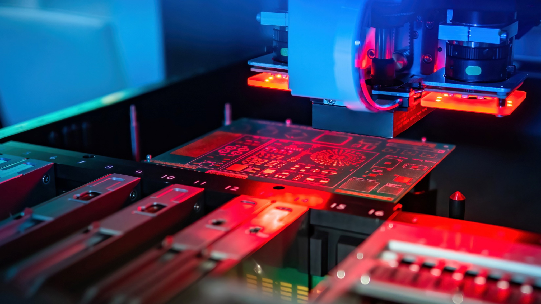
PCB electrical simulation refers to the process of simulating and analyzing the behavior of a printed circuit board (PCB) through software. Various software tools are used to simulate the electrical performance of the PCB, allowing for the identification of potential issues before entering the manufacturing process. It helps in further problem-solving, design optimization, and improvement. For example, simulations can evaluate the board's response to different voltages, currents, and frequencies. By simulating the behavior of PCB, engineers can identify issues and improve the performance and reliability of the circuit board.
Inside of PCIe - PCB Validation
PCIe 5.0 Electrical Testing
In the PCB industry, there are various methods for PCB electrical testing. The traditional mainstream methods include SET2DIL (Single-Ended TDR to Differential insertion loss) and SPP (Short Pulse Propagation). However, these two methods are subject to the parasitic effects of parasitic capacitance and inductance in the Via and Via Stub, which can lead to inaccurate measurements at high frequencies. Intel has therefore developed the Delta-L analysis method, which eliminates the complex calibration steps and deducts the parasitic effect, and has developed a proprietary probe head in conjunction with a tool supplier to establish a standard PCB material loss per Inch measurement method. USI has implemented this measurement process, which helps ensure product quality and the detection of final products in the high-speed transmission interface design field.
Learn More:Get a head start for AI at the edge
With years of design experience in cloud and storage devices, USI offers comprehensive design and electrical simulation services during PCB design. Utilizing 3D electromagnetic field simulation software, USI optimizes PCB impedance to minimize the impact of multiple reflections on signals. Additionally, USI employs time-domain circuit analysis tools to effectively address issues related to interference, attenuation, crosstalk, and other related problems, ensuring that the terminal signals meet the standard specifications of PCI-SIG.
PCB High-Speed Signal Design Verification & Simulation
The automated Front-End Design Simulation which developed by USI has been successfully applied to the design guidelines of major chip manufacturers (Intel, AMD, Qualcomm, MTK...etc.) to ensure the design accuracy of power integrity. In addition, we have also developed an automatic PCB routing design check Rule, which not only effectively replaces the tedious manual checks and greatly reduces the development time but also brings fast and excellent PCB routing quality. For example, most servers have 2,000-5,000 signal lines and it is difficult to verify the quality of the wiring with the human eye, so an automated inspection can ensure and improve the quality of the PCB wiring.
Future Trend of PCIe
The future of PCIe is focused on increasing bandwidth and data transfer speeds, and at the 2021 Developer Conference, PCI-SIG officially announced the PCI 6.0 specification, which changes the modulation technology from NRZ (Non-Return-to-Zero) to PAM4 (Pulse Amplitude Modulation), allowing transfer rates of up to 64 GT/s. PCIe 6.0 also introduces features such as PAM4 coding, which enables signalling levels to increase data transfer rates, and low latency Forward Error Correction (FEC). s. PCIe 6.0 also introduces new features such as PAM4 coding, which enables quadruple signalling to increase data transfer rates, and low-latency Forward Error Correction (FEC), which improves error detection and correction for faster and more reliable data transfer. In the following year (2022), the PCIe 7.0 standard is being developed, allowing transfer rates to double again to a high performance of 128 GT/s.
Learn More:Fleet management: Invisible Hands Drive Your Team Wisely
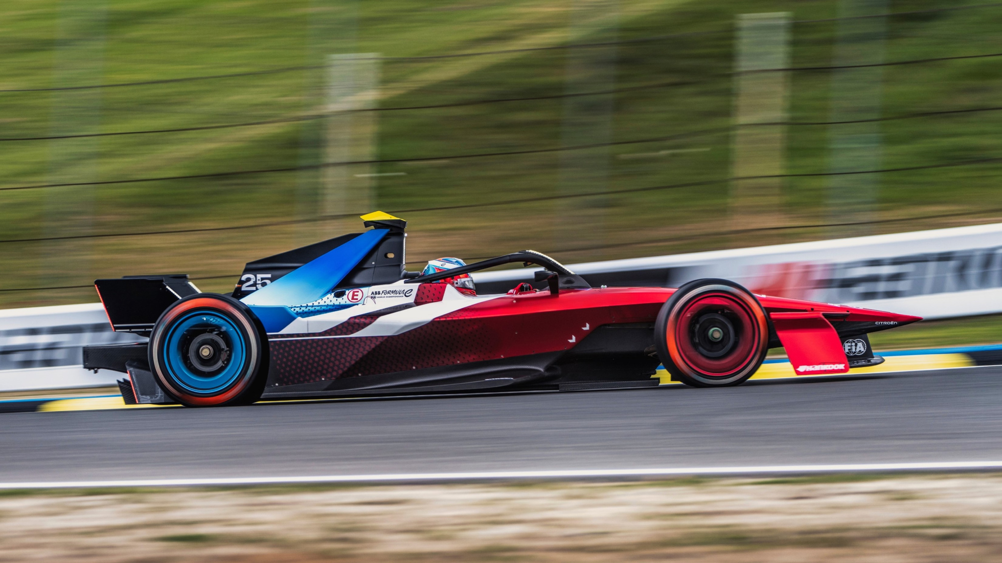
Another trend is the increasing use of PCIe in new applications such as automotive and industrial systems. These systems require high-speed data transfer and real-time processing, making PCIe an ideal choice for their communication and control systems. The combination of PCIe 5.0 and PCB simulation technology can provide higher performance and faster data processing speeds for next-generation technologies.
Designers can use these technologies to reduce design flaws, improve system performance, and bring new products to market in shorter timeframes. Although it will take some time before the PCIe 5.0 is ready for mass introduction into the consumer market, USI will continue to refine the design and optimization of high-speed interface-related technologies to meet customer needs with highly competitive products.
FAQs
1. What is the difference between PCIe 5.0 and PCIe 4.0?
PCIe 5.0 provides higher data transfer speeds and bandwidth than PCIe 4.0. This makes PCIe 5.0 more suitable for handling massive data and real-time applications.
2. What can PCB simulation technology help me do?
Using PCB simulation technology, you can better understand potential design issues and optimize them before actual production. This helps to improve system performance, reduce costs, and save time.
3. Is PCB electrical loss testing necessary?
Yes, by measuring the electrical loss of the PCB, it is possible to assess the signal degradation in the PCB traces and determine if further design optimisation measures are required, such as changing the PCB material, tracing layout or adopting enhanced signal transmission techniques. When PCIe 5.0 transfer speeds reach 32 GT/s, electrical loss testing became an essential process.
4. Can PCB simulation technology detect all design flaws?
PCB simulation technology can detect most design flaws but is not foolproof. Using a combination of simulation and physical testing is important to ensure that your design is optimized for performance and reliability.
5. How is automated inspection and simulation for PCB high-speed signal design different from the past?
Most servers use Intel or AMD platforms with 2,000-5,000 signal lines, making it difficult to verify the quality of the alignment with the human eye. Therefore, by developing and implementing automated inspection, the PCB routing quality can be improved. Power integrity simulations can only be performed when the PCB design is almost complete, and the simulations require a certain amount of manual time to set up, so the introduction of power integrity simulation automation can optimize the power design to meet the design objectives and ensure that the chipsets can work properly within a limited time frame.
Contact USI Design Team here if you require more professional details.
Search
Recent Articles
-
When AI Learns to “Read”: Using Deep Learning to Tame the False-Alarm Storm on SMT Production Lines
 When AI Learns to “Read”: Using Deep Learning to Tame the False-Alarm Storm on SMT Production Lines
07/13/2026
When AI Learns to “Read”: Using Deep Learning to Tame the False-Alarm Storm on SMT Production Lines
07/13/2026
-
Catching Invisible “Micro-Failures”: Safeguarding SiP Reliability Testing with Daisy Chains
 Catching Invisible “Micro-Failures”: Safeguarding SiP Reliability Testing with Daisy Chains
06/29/2026
Catching Invisible “Micro-Failures”: Safeguarding SiP Reliability Testing with Daisy Chains
06/29/2026
-
The Hidden Rival Inside an EV’s Heart: Cracking the Power-Loss Puzzle with “Physical Modeling”
 The Hidden Rival Inside an EV’s Heart: Cracking the Power-Loss Puzzle with “Physical Modeling”
06/17/2026
The Hidden Rival Inside an EV’s Heart: Cracking the Power-Loss Puzzle with “Physical Modeling”
06/17/2026
-
Behind the MFG. | From "Manufacturing" to "Creation" Ep.2: Innovation Built from Zero to One
 Behind the MFG. | From "Manufacturing" to "Creation" Ep.2: Innovation Built from Zero to One
05/28/2026
Behind the MFG. | From "Manufacturing" to "Creation" Ep.2: Innovation Built from Zero to One
05/28/2026
-
Behind the MFG. | From "Manufacturing" to "Creation" Ep.1: Unveiling USI’s Technological Vanguard
 Behind the MFG. | From "Manufacturing" to "Creation" Ep.1: Unveiling USI’s Technological Vanguard
05/07/2026
Behind the MFG. | From "Manufacturing" to "Creation" Ep.1: Unveiling USI’s Technological Vanguard
05/07/2026
-
Breaking the AI Energy Wall: Power Block and 3D Miniaturization Solutions
 Breaking the AI Energy Wall: Power Block and 3D Miniaturization Solutions
12/31/2025
Breaking the AI Energy Wall: Power Block and 3D Miniaturization Solutions
12/31/2025
-
Mastering Automotive HPC: Defining the "Sweet Spot" of SoMoG Technology
 Mastering Automotive HPC: Defining the "Sweet Spot" of SoMoG Technology
12/15/2025
Mastering Automotive HPC: Defining the "Sweet Spot" of SoMoG Technology
12/15/2025
-
【Smart Power Supply】Innovative Solution for DAC Control Bias Current
 【Smart Power Supply】Innovative Solution for DAC Control Bias Current
10/21/2025
【Smart Power Supply】Innovative Solution for DAC Control Bias Current
10/21/2025
-
From Experience to Precision: How AI Algorithms Enable Efficient RF Prediction Models
 From Experience to Precision: How AI Algorithms Enable Efficient RF Prediction Models
09/11/2025
From Experience to Precision: How AI Algorithms Enable Efficient RF Prediction Models
09/11/2025
-
Event|DIGITIMES 2025 D Forum – USI Shares How Heterogeneous Integration Drives a New Landscape for MCU Applications
 Event|DIGITIMES 2025 D Forum – USI Shares How Heterogeneous Integration Drives a New Landscape for MCU Applications
08/15/2025
Event|DIGITIMES 2025 D Forum – USI Shares How Heterogeneous Integration Drives a New Landscape for MCU Applications
08/15/2025
Keep up with top trending topic
For the latest innovation technology, application
and industry insight.
Subscribe Our Blog
For the latest innovation technology, application
and industry insight.