USI Blog
Top trending topic for the latest innovation technology, application and industry insight.
Search
- 04/02/2024
Breaking the Size Barrier : Mastering the Art of Miniaturization
The miniaturization of electronics requires smaller, more efficient packaging solutions, and the field encompasses a variety of ways to achieve miniaturization. This advanced packaging technology integrates multiple dies, active, passive components, and even electromechanical devices into a single miniaturized package. This integration offers significant advantages in terms of size reduction, performance enhancement, and overall system functionality. Before start it, you can get more about SiP technology from our another article: System in Package (SiP) for Miniaturization: Turnkey Solution We Offer
In this article, let’s dive into the world of System-in-Package (SiP), explore its intricate assembly process and other advanced packaging solutions like System-in-Package (SiP), System-on-Chip (SoC), and Chiplet.
Break Down the SiP Assembly Steps
The SiP manufacturing process involves several key steps, by following these meticulous steps, manufacturers can ensure the quality, reliability, and long-term functionality of SiP modules used in various electronic devices:
- Substrate preparation
- The selected substrate undergoes a surface treatment process to ensure proper adhesion of components. This process is often handled by the PCB manufacturer before passing on to the packaging manufacturer. It may involve cleaning, roughening the surface, and applying a thin layer of metal (usually copper) for better conductivity.
- Stencils, which are metallic sheets with laser-cut holes to match the size and location of component footprints, are placed on the prepared substrate.
- Solder paste, a viscous material containing tiny solder powders, will be printed onto the designated areas of the substrate through the stencil openings, creating solder pads for component attachment.
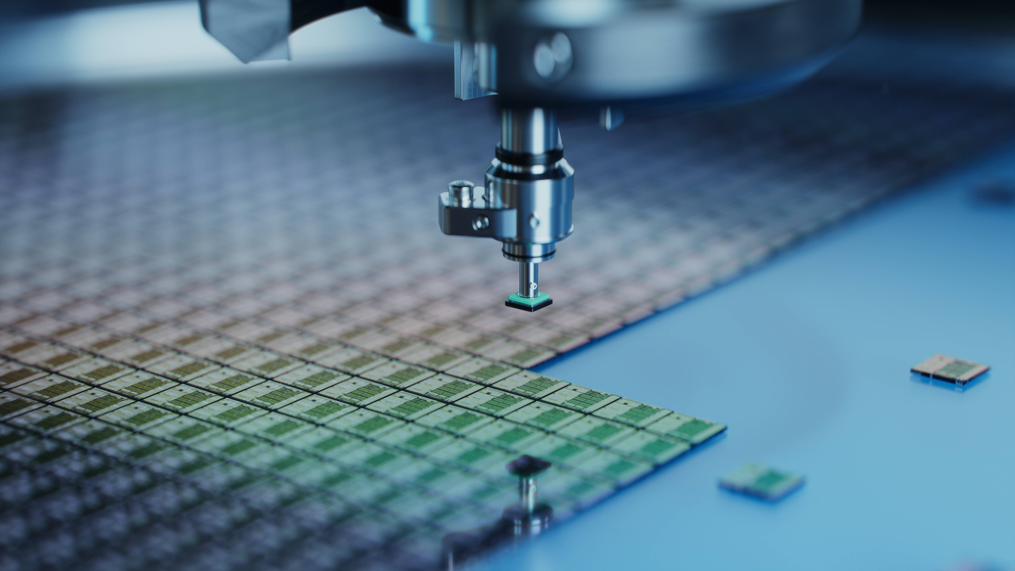
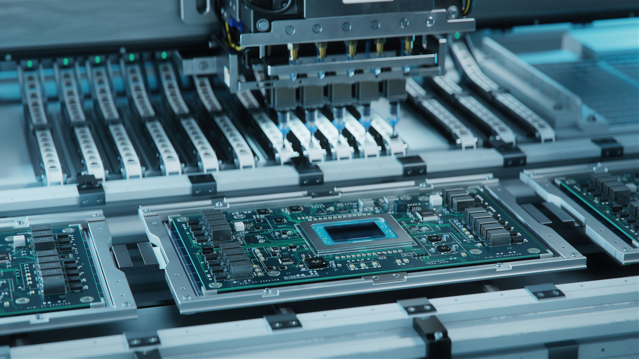
- High-Density Surface Mount Technology (HD-SMT)
After the solder paste is printed on the surface of the substrate, the next step is to place the solder feet of the electronic components on the solder paste. At this stage, the high-precision Chip mounter equipped with adsorption nozzles and vision systems come into play. These machines pick individual components from reels or tray feeder and precisely place them on the substrate. The accuracy of this process is crucial, as misalignment can lead to electrical connection failures. Then, high temperature is used to melt the solder paste and solder the electronic components on the substrate.
Get to Know More: USI SiP Technology - High Density SMT
Get to Know More: USI SiP Technology - High Density SMT
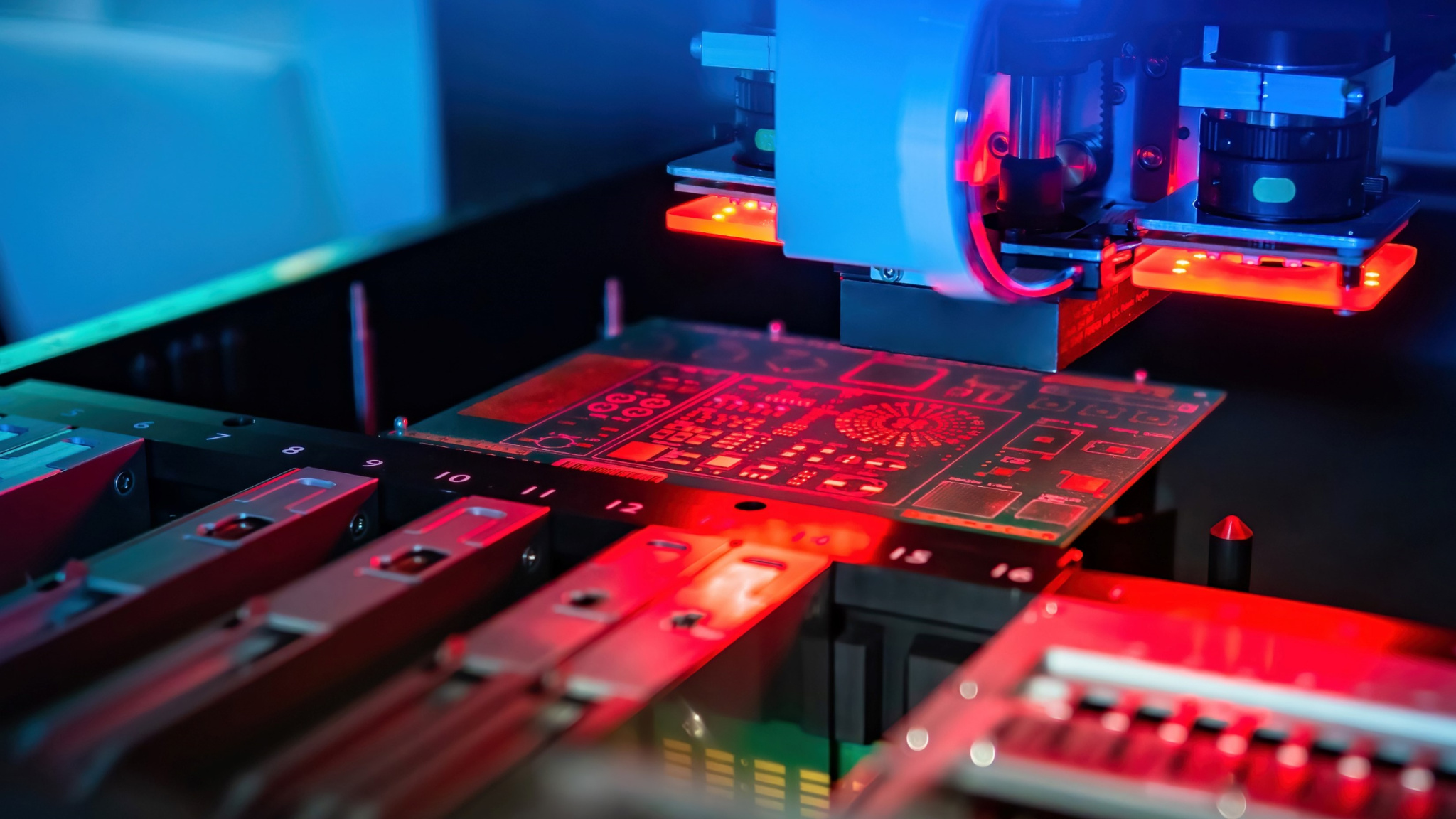
- Interconnection through Die / Wire Bonding
For use in higher-end miniaturized products, the other two technologies are needed to allow the components on these circuit boards to "communicate" with each other: die bonding and wire bonding. The process “Die Bonding” will continue to attach unpackaged integrated circuits (ICs), or "dies," to the substrate with miniscule amount of conductive adhesive placed on the substrate, and then the die is meticulously positioned and secured using intense pressure and heat. This forms an enduring, rock-solid connection between the die and the substrate.
Another method, wire bonding, employs microscopic metallic wires, typically copper, gold or aluminum, to establish electrical connections throughout the SiP module. It utilizes a bonding capillary or ball bonding process to meticulously attach these wires to designated bonding pads. Wire bonding offers adaptability when routing these intricate connections, making it ideal for components with varying heights.
Another method, wire bonding, employs microscopic metallic wires, typically copper, gold or aluminum, to establish electrical connections throughout the SiP module. It utilizes a bonding capillary or ball bonding process to meticulously attach these wires to designated bonding pads. Wire bonding offers adaptability when routing these intricate connections, making it ideal for components with varying heights.
- Encapsulation
Once the electrical connections are formed, the entire SiP module is encapsulated with a protective material, typically the epoxy resins. This protects the delicate components from environmental factors like moisture, dust, and physical impact. Different encapsulation techniques may be employed from different demands, alongside full body encapsulation (covering the entire SiP module), selective and stepped encapsulation are also possible.
Here you can get to Know More: USI SiP Technology – Molding , USI SiP Technology – Shielding
Here you can get to Know More: USI SiP Technology – Molding , USI SiP Technology – Shielding
- Testing and inspection
After encapsulation, the SiP module will undergo rigorous testing to ensure its functionality and performance. This may involve electrical testing to verify proper connections and component operation, as well as optical and X-ray inspections to detect any defects or voids within the encapsulation material. Functional testing simulates the real operation environment to evaluate the overall performance of the SiP module.
The Beauty of SiP Manufacturing Process
SiP technology offers several compelling advantages:
- Compact Design: By integrating multiple components, SiP significantly reduces the overall footprint of electronic devices. This is crucial for consumer applications where space is a premium, such as wearable electronics and smartphones.
- Improved Performance: SiP enables shorter electrical paths between components, leading to faster signal transmission and better signal integrity. This translates to enhanced system performance.
- Increased Reliability: SiP can improve the reliability of electronic devices by the packaging technologies to protect components from external stress, moisture, and contaminants like dust.
- Faster Time-to-Market: By integrating components in the modular design, SiP can streamline simultaneous multiple product development and shorten the time to bring the products to market. This allows brand owners, which are our customers, to capitalize on market opportunities more quickly.
What Miniaturization Solutions other than SiP?
System-in-Package (SiP) technology is one of solutions to revolutionize the electronics industry by enabling the miniaturization and integration of complex functionalities. But which solution will be chosen that can be diversity regarding customers, products and even the budgets. So, let's look at the other two packaging solutions that are highly discussed in the market today:
USI Tech Discovery | The Nature of Miniaturization Technology: SoC、Chiplet、SiP
SoC (System on Chip)
SoC involves the integration of diverse functionalities onto a single chip, encompassing crucial components such as processors, memory units, and input/output interfaces. This consolidation of functions onto a unified platform streamlines the architecture of electronic systems, leading to enhanced efficiency and reduced footprint. However, even though SoC technology is still widely adopted by the mainstream market, it is inevitable that more new functional units will need to be integrated in the face of ever-changing functional requirements. In the face of this problem, SoC technology has begun to show process bottlenecks.
What would be the Challenges be?
One of the primary obstacles is its rigid nature in manufacturing, which limits the agility of the chip in accommodating dynamic requirements. Although SoC technology is capable of integrating different functions, it is limited to components of the same technology level. This inflexibility often necessitates substantial redesign efforts in response to modifications or upgrades, resulting in delays and increased development expenditures. These challenges underscore the importance of alternative miniaturization technologies, such as Chiplet and System-in-Package (SiP).
Chiplet
With the rapid rise of AI applications around the world in recent years, the demand for highly computational and image-processing modules has begun to increase dramatically, and Chiplet technology has become the first choice for AI applications. Because chiplet technology offers greater design flexibility than System-on-chip (SoC). Unlike SoCs, where all components are confined to the same process, Chiplets enable the assembly of different components using diverse processes onto a single interposer layer. This flexibility makes Chiplet technology a compelling option for high-performance computing tasks such as those required in AI applications.
What would be the Challenges?
The main difficulties of Chiplet technology will center around production yield and cost. The intricate process of assembling multiple dies onto an interposer layer demands precise manufacturing techniques, which can increase the likelihood of defects and raise production costs. Additionally, managing thermal dissipation and power distribution across multiple chiplets within a compact package presents another obstacle, as increased power density could exacerbate heat dissipation challenges and compromise overall system reliability. Despite these challenges, packaging technologies are steadily addressing these issues, paving the way for the widespread adoption of Chiplet technology across diverse applications, including AI, high-performance computing, and beyond.
There is a diversity of advanced packaging solutions that can be chosen, depending on the product’s performance requirements. While each solution offers unique advantages, SiP emerges as a compelling choice for many applications. It strikes a remarkable balance between miniaturization, functionality, and cost. When considering all factors, SiP stands out as a mature, versatile, and cost-effective solution for a wide range of applications.
Search
Recent Articles
-
When AI Learns to “Read”: Using Deep Learning to Tame the False-Alarm Storm on SMT Production Lines
 When AI Learns to “Read”: Using Deep Learning to Tame the False-Alarm Storm on SMT Production Lines
07/13/2026
When AI Learns to “Read”: Using Deep Learning to Tame the False-Alarm Storm on SMT Production Lines
07/13/2026
-
Catching Invisible “Micro-Failures”: Safeguarding SiP Reliability Testing with Daisy Chains
 Catching Invisible “Micro-Failures”: Safeguarding SiP Reliability Testing with Daisy Chains
06/29/2026
Catching Invisible “Micro-Failures”: Safeguarding SiP Reliability Testing with Daisy Chains
06/29/2026
-
The Hidden Rival Inside an EV’s Heart: Cracking the Power-Loss Puzzle with “Physical Modeling”
 The Hidden Rival Inside an EV’s Heart: Cracking the Power-Loss Puzzle with “Physical Modeling”
06/17/2026
The Hidden Rival Inside an EV’s Heart: Cracking the Power-Loss Puzzle with “Physical Modeling”
06/17/2026
-
Behind the MFG. | From "Manufacturing" to "Creation" Ep.2: Innovation Built from Zero to One
 Behind the MFG. | From "Manufacturing" to "Creation" Ep.2: Innovation Built from Zero to One
05/28/2026
Behind the MFG. | From "Manufacturing" to "Creation" Ep.2: Innovation Built from Zero to One
05/28/2026
-
Behind the MFG. | From "Manufacturing" to "Creation" Ep.1: Unveiling USI’s Technological Vanguard
 Behind the MFG. | From "Manufacturing" to "Creation" Ep.1: Unveiling USI’s Technological Vanguard
05/07/2026
Behind the MFG. | From "Manufacturing" to "Creation" Ep.1: Unveiling USI’s Technological Vanguard
05/07/2026
-
Breaking the AI Energy Wall: Power Block and 3D Miniaturization Solutions
 Breaking the AI Energy Wall: Power Block and 3D Miniaturization Solutions
12/31/2025
Breaking the AI Energy Wall: Power Block and 3D Miniaturization Solutions
12/31/2025
-
Mastering Automotive HPC: Defining the "Sweet Spot" of SoMoG Technology
 Mastering Automotive HPC: Defining the "Sweet Spot" of SoMoG Technology
12/15/2025
Mastering Automotive HPC: Defining the "Sweet Spot" of SoMoG Technology
12/15/2025
-
【Smart Power Supply】Innovative Solution for DAC Control Bias Current
 【Smart Power Supply】Innovative Solution for DAC Control Bias Current
10/21/2025
【Smart Power Supply】Innovative Solution for DAC Control Bias Current
10/21/2025
-
From Experience to Precision: How AI Algorithms Enable Efficient RF Prediction Models
 From Experience to Precision: How AI Algorithms Enable Efficient RF Prediction Models
09/11/2025
From Experience to Precision: How AI Algorithms Enable Efficient RF Prediction Models
09/11/2025
-
Event|DIGITIMES 2025 D Forum – USI Shares How Heterogeneous Integration Drives a New Landscape for MCU Applications
 Event|DIGITIMES 2025 D Forum – USI Shares How Heterogeneous Integration Drives a New Landscape for MCU Applications
08/15/2025
Event|DIGITIMES 2025 D Forum – USI Shares How Heterogeneous Integration Drives a New Landscape for MCU Applications
08/15/2025
Keep up with top trending topic
For the latest innovation technology, application
and industry insight.
Subscribe Our Blog
For the latest innovation technology, application
and industry insight.