USI Blog
Top trending topic for the latest innovation technology, application and industry insight.
Search
- 04/24/2023
System in Package (SiP) for Miniaturization: Turnkey Solution We Offer
As the demand for various consumer communication products increases, semiconductor components must be more versatile and require system integration between components. Due to bottlenecks in semiconductor process technology, system-on-chip (SoC) development becomes less efficient, more challenging to integrate heterogeneously, and more costly and time-consuming. This is where the System-in-Package (SiP) market opportunity begins to emerge.
Advantages of adopting System in Package (SiP)
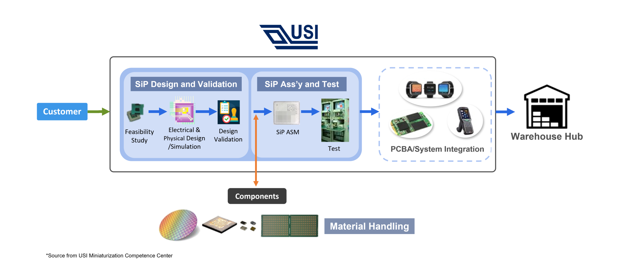
USI Turnkey Service for System in Package
The key advantage of adopting System-in-Package (SiP) over SoC is that it can be freely combined according to the functions and requirements, providing customers with flexible designs. Take the most common smartphone as an example. Common functional modules include sensors, Wi-Fi, BT/BLE, RF FEM, power management chips, etc. System-in-package is the integration of these individually manufactured chips and components into modules, and then from a single functional module into a sub-system, the system is then mounted on the handset system PCB.
The SiP process covers crystal, wire bonding, active/passive component SMT, and encapsulation technology. The packaging shape can be designed and produced according to customer design, even in a 3D structure. This can reduce the overall size, leave more space for batteries, provide larger power storage, extend product usage time, and make the mobile phone work faster with more functions. Therefore, it is particularly suitable for radio frequency-related applications such as 5G millimeter-wave modules, UWB, and other fields.
Three Critical Technologies Among SiP Processes
The number and spacing of components in the PCB design is the primary key to the module size. To achieve miniaturization, there are three critical technologies among SiP processes: encapsulation, shielding and high-density SMT.
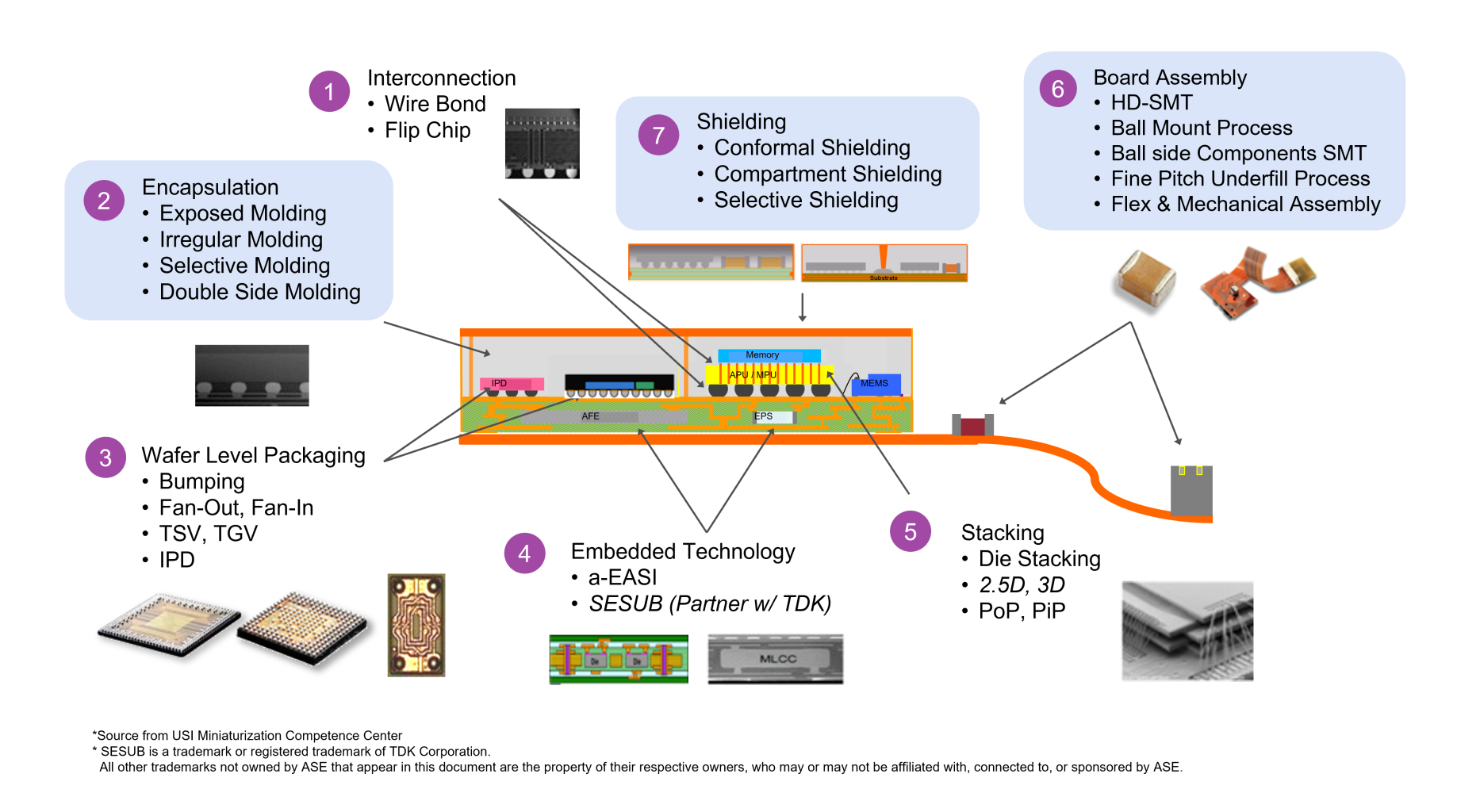
Key Process Technology for System in Package
High-Density SMT
Regarding high-density laminating processes, USI has achieved 40μm of the diameter of a baby's hair. Compared to the 10x10 array, over 70% of the board size is significantly reduced, 40% of which is due to breakthroughs in lamination technology.
Encapsulation
Since the high-density SMT process uses miniaturized components, the connection with the substrate is significantly reduced in solder connection. In order to improve the components’ reliability and to avoid the influence of external humidity, high temperature and pressure, the molding process allows the complete components to be sealed and wrapped on the substrate. Outsourcing and testing (OSAT) in highly integrated system packaging can achieve about 100 components into a module, while USI can accommodate up to 900 components.
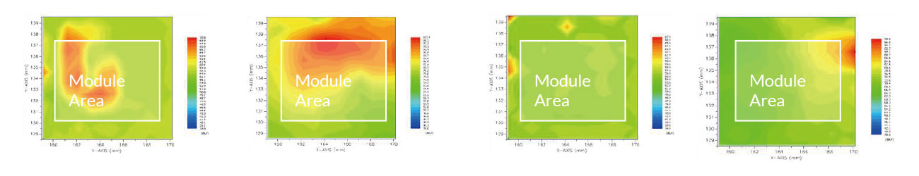
Conformal & Compartment Shielding
On the other hand, SiP modules require high-density integration of hundreds of electronic components while avoiding interference with other components on the PCB board. In addition, the same interference problem must be solved outside the module. Therefore, an important process is required to create a barrier between components, known as Conformal Shielding and Compartment Shielding.
While the industry's most common metal shields require approximately 1mm of solder pads and a Keep-Out Zone for each section, USI’s shielding process requires only 10% of the width. Take a multi-frequency 4G module, for example; it can free up more than 17% of the space for other components and can be shielded from electromagnetic interference by 40-50 dB.
Turnkey Services in System in Package (SiP)
With more than ten years of experience, USI has made breakthroughs in key processand provided customers with " Turnkey Services in System-in-Package". From SiP design for EE/RF, board-level and module simulation, verification, process, system-level testing, and even material control and delivery of finished products to designated warehouses, we are able to meet the diverse needs of our customers.
USI SiP Experience – Applications
To meet our customers' design needs for SiP, we have a comprehensive database that provides the best solution in terms of components and design based on miniaturization, followed by the layout and structure design. Through SiP technology, the entire circuit and subsystem will be molded into a module that is only the size of a 'wafer'.
Simulation and verification of high-density and highly integrated modular designs are particularly important in the early stages. USI provides services such as carrier board design and warpage simulation, power/signal integrity analysis (PI/SI) and thermal simulation (Thermal) to ensure the quality of module design. The lab is also fully equipped for system integration verification, assisting customers with RF calibration tests and protocol verification after the modules are pasted onto the board, as well as providing system-level functionality and reliability verification.
Reliability and Failure Analysis for SiP Modules
When problems arise in the module, it becomes increasingly difficult to analyze the abnormalities of its micrometer-level components. Furthermore, the complex connections between the internal trace and substrate make it particularly challenging to determine the problem, especially during electrical testing when other components can affect the results.
Additionally, some abnormal contaminations may only have a few nanometers of thickness, such as oxidation or micro-erosion, which cannot be detected by conventional optical or electron microscopes. In order to minimize process issues, USI continually strengthens its analytical capabilities in the field of SiP module failure analysis, utilizing three major quality control instruments: 3D X-ray inspection, X-ray photoelectron spectroscopy (XPS), and Fourier transform infrared spectroscopy (FTIR), to find solutions through the following three steps:
Three Steps of Failure Analysis
- 3D X-ray Inspection: Through X-ray inspection in the failure analysis, we can accurately identify if the module has any assembly abnormalities and locate the position of the abnormal component.
- X-ray Photoelectron Spectroscopy (XPS): Next, we use XPS to conduct more detailed element analysis on the micrometer-level surface of the module, exploring whether electrical abnormalities, high resistance values, ball planting or dropping, or sputter layer delamination phenomena are caused by oxidation or contamination in the manufacturing process.
- Fourier Transform Infrared Spectroscopy (FTIR): If the target contaminant is clearly identified, we can then use FTIR to identify organic contaminants and define the root cause of the problem, thereby finding the correct solution.
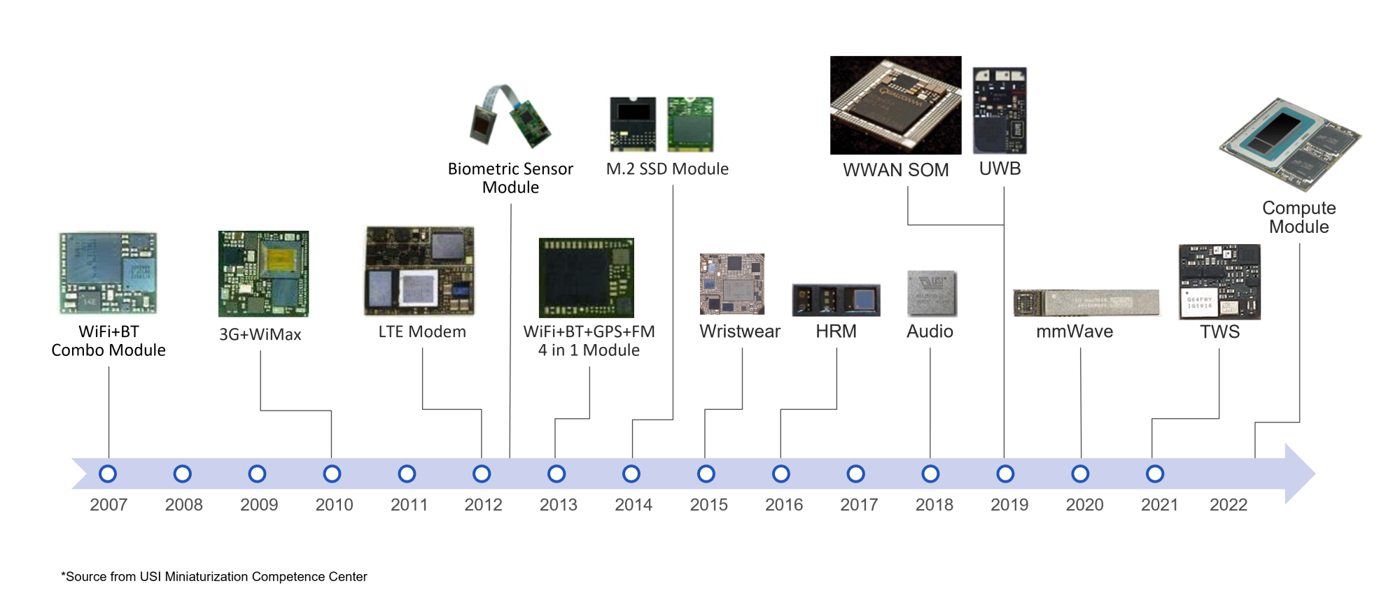
Breakthrough in the Miniaturization Competition
With the advantage of heterogeneous integration and miniaturization, system-level packaging can integrate components from different process technology nodes, different functions, different suppliers and even different semiconductor raw materials, saving about 30-40% of the overall product space. It is also possible to customize module shapes and simplify the board design to a certain extent, allowing more flexibility in the integration of board, antenna, and mechanism design.
At the same time, system integration modules can be validated and certified at the system level compared to the limitations of IC process development, speeding up end product development and concentrating system product development resources.
SiP technology is the focus of the global packaging industry, and breakthroughs in system-in-package (SiP) technology are affecting the supply chain and changing the competitive landscape. With years of experience in RF and wearable devices, USI now is able to help customers realize ideas through our " Turnkey Services in System in Package ".
Excerpts from the NEPCON Speech by Hsin Huang, Associate Technical Director of USI Miniaturization Competence Center, 2022.06.30
Search
Recent Articles
-
When AI Learns to “Read”: Using Deep Learning to Tame the False-Alarm Storm on SMT Production Lines
 When AI Learns to “Read”: Using Deep Learning to Tame the False-Alarm Storm on SMT Production Lines
07/13/2026
When AI Learns to “Read”: Using Deep Learning to Tame the False-Alarm Storm on SMT Production Lines
07/13/2026
-
Catching Invisible “Micro-Failures”: Safeguarding SiP Reliability Testing with Daisy Chains
 Catching Invisible “Micro-Failures”: Safeguarding SiP Reliability Testing with Daisy Chains
06/29/2026
Catching Invisible “Micro-Failures”: Safeguarding SiP Reliability Testing with Daisy Chains
06/29/2026
-
The Hidden Rival Inside an EV’s Heart: Cracking the Power-Loss Puzzle with “Physical Modeling”
 The Hidden Rival Inside an EV’s Heart: Cracking the Power-Loss Puzzle with “Physical Modeling”
06/17/2026
The Hidden Rival Inside an EV’s Heart: Cracking the Power-Loss Puzzle with “Physical Modeling”
06/17/2026
-
Behind the MFG. | From "Manufacturing" to "Creation" Ep.2: Innovation Built from Zero to One
 Behind the MFG. | From "Manufacturing" to "Creation" Ep.2: Innovation Built from Zero to One
05/28/2026
Behind the MFG. | From "Manufacturing" to "Creation" Ep.2: Innovation Built from Zero to One
05/28/2026
-
Behind the MFG. | From "Manufacturing" to "Creation" Ep.1: Unveiling USI’s Technological Vanguard
 Behind the MFG. | From "Manufacturing" to "Creation" Ep.1: Unveiling USI’s Technological Vanguard
05/07/2026
Behind the MFG. | From "Manufacturing" to "Creation" Ep.1: Unveiling USI’s Technological Vanguard
05/07/2026
-
Breaking the AI Energy Wall: Power Block and 3D Miniaturization Solutions
 Breaking the AI Energy Wall: Power Block and 3D Miniaturization Solutions
12/31/2025
Breaking the AI Energy Wall: Power Block and 3D Miniaturization Solutions
12/31/2025
-
Mastering Automotive HPC: Defining the "Sweet Spot" of SoMoG Technology
 Mastering Automotive HPC: Defining the "Sweet Spot" of SoMoG Technology
12/15/2025
Mastering Automotive HPC: Defining the "Sweet Spot" of SoMoG Technology
12/15/2025
-
【Smart Power Supply】Innovative Solution for DAC Control Bias Current
 【Smart Power Supply】Innovative Solution for DAC Control Bias Current
10/21/2025
【Smart Power Supply】Innovative Solution for DAC Control Bias Current
10/21/2025
-
From Experience to Precision: How AI Algorithms Enable Efficient RF Prediction Models
 From Experience to Precision: How AI Algorithms Enable Efficient RF Prediction Models
09/11/2025
From Experience to Precision: How AI Algorithms Enable Efficient RF Prediction Models
09/11/2025
-
Event|DIGITIMES 2025 D Forum – USI Shares How Heterogeneous Integration Drives a New Landscape for MCU Applications
 Event|DIGITIMES 2025 D Forum – USI Shares How Heterogeneous Integration Drives a New Landscape for MCU Applications
08/15/2025
Event|DIGITIMES 2025 D Forum – USI Shares How Heterogeneous Integration Drives a New Landscape for MCU Applications
08/15/2025
Keep up with top trending topic
For the latest innovation technology, application
and industry insight.
Subscribe Our Blog
For the latest innovation technology, application
and industry insight.