USI Blog
Top trending topic for the latest innovation technology, application and industry insight.
Search
- 06/17/2026
The Hidden Rival Inside an EV’s Heart: Cracking the Power-Loss Puzzle with “Physical Modeling”

Authors: Albert Lin, Jack Chen, Bob Jan, Rick Lin / Advanced Power Module R&D Team
The rise of electric vehicles is putting a single component ”the power module” squarely in the industry spotlight. It is the core of an EV’s traction inverter, responsible for converting the battery’s direct current (DC) into the alternating current (AC) that drives the motor. In recent years, power modules built on silicon carbide (SiC) semiconductors have been regarded as key to extending EV range and performance, thanks to their faster switching speed and higher efficiency, where every additional percentage point of efficiency can decide a win or a loss. Speed, however, is a double-edged sword: SiC is extremely sensitive to the “parasitic effects” introduced by the PCB layout. A single invisible parasitic inductance can quietly turn the energy that should have been saved back into wasted heat.
Learn More:What you should not miss about IGBT and SiC in EV Power Module
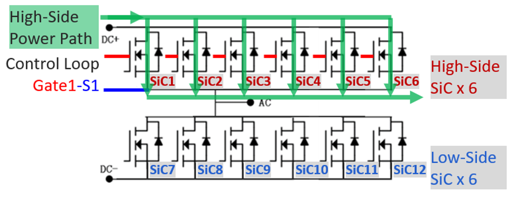
Fig.1 | The power module in this case comprises 12 SiC devices, with the power path and control loop interwoven across the layout.
A First JDM Power Module — Meeting a “Doubled” Switching Loss
In USI’s first power-module JDM (Joint Design and Manufacturing) project, we met this challenge head-on. It was a power module co-developed with a customer for a high-performance racing application, using the latest SiC technology. Notably, in a conventional IGBT, switching loss accounts for roughly 80% of total loss; switching to SiC can bring that share down to about 50%, which is precisely why the industry is moving aggressively toward SiC. But this holds only if the layout is “clean” enough—otherwise parasitic effects can swallow SiC’s advantage whole.
Sure enough, initial simulations showed that once the PCB layout’s influence was included, the high-side switching loss surged to nearly double the ideal baseline, far beyond the customer’s expectations. Left unresolved, the power module would overheat severely under high load, driving up cooling costs, reducing reliability, and even jeopardizing the shipment schedule. The customer’s requirement was clear: identify the root cause and deliver a concrete, quantifiable improvement plan.
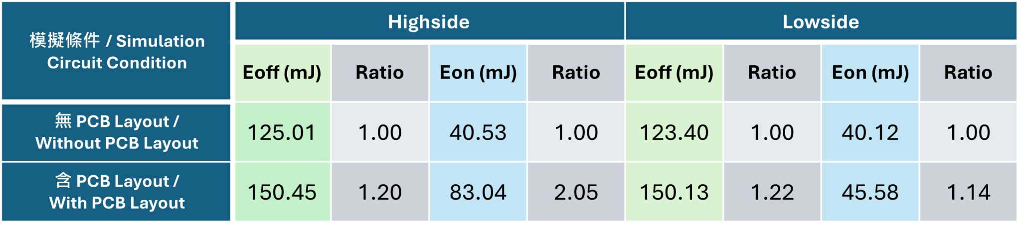
Fig.2 | After including the PCB layout, the high-side turn-on loss (Eon) jumps to 2.05× the baseline—far higher than on the low side.
Why Can’t Conventional Simulation Catch the Culprit?
The problem is that conventional design flows rely mainly on “numerical modeling.” These software-generated models are accurate, yet they behave like a “black box”, they can tell you the result is off, but they cannot pinpoint which copper trace or which bonding wire on the actual PCB is the source of the trouble. Engineers can see the anomaly but cannot catch the culprit; all they can do is revise the layout and rerun simulations over and over, time-consuming and hard to converge. This is the biggest pain point in many power-module development projects: you know the patient is “sick,” yet you cannot find the “lesion.”
Borrowing a Trick from RF Engineering: “Drawing” the Circuit Back onto the PCB
To break through this bottleneck, we adopted a method long established in radio-frequency (RF) engineering but relatively uncommon in power-module design: “physical modeling.” Its essence is to “draw” the equivalent circuit back onto the physical structure according to the actual current paths on the PCB layout, so that every inductance and resistance corresponds to a specific location on the layout. We focused in particular on the “shared path” where the control loop and the power path overlap, because this is exactly where the shared-path parasitic inductance (Ls) most easily causes trouble. Since the energy of the switching transient is concentrated in the rapid change of current, we placed our analytical emphasis on series parasitic inductance rather than shunt capacitance, keeping the model focused on the key physics without becoming overly complex. To obtain precise values, we used ANSYS Q3D to extract the PCB’s S-parameter model and, based on the roughly 10 MHz frequency of the switching transient, calculated the parasitic resistance and inductance of each path, segment by segment.
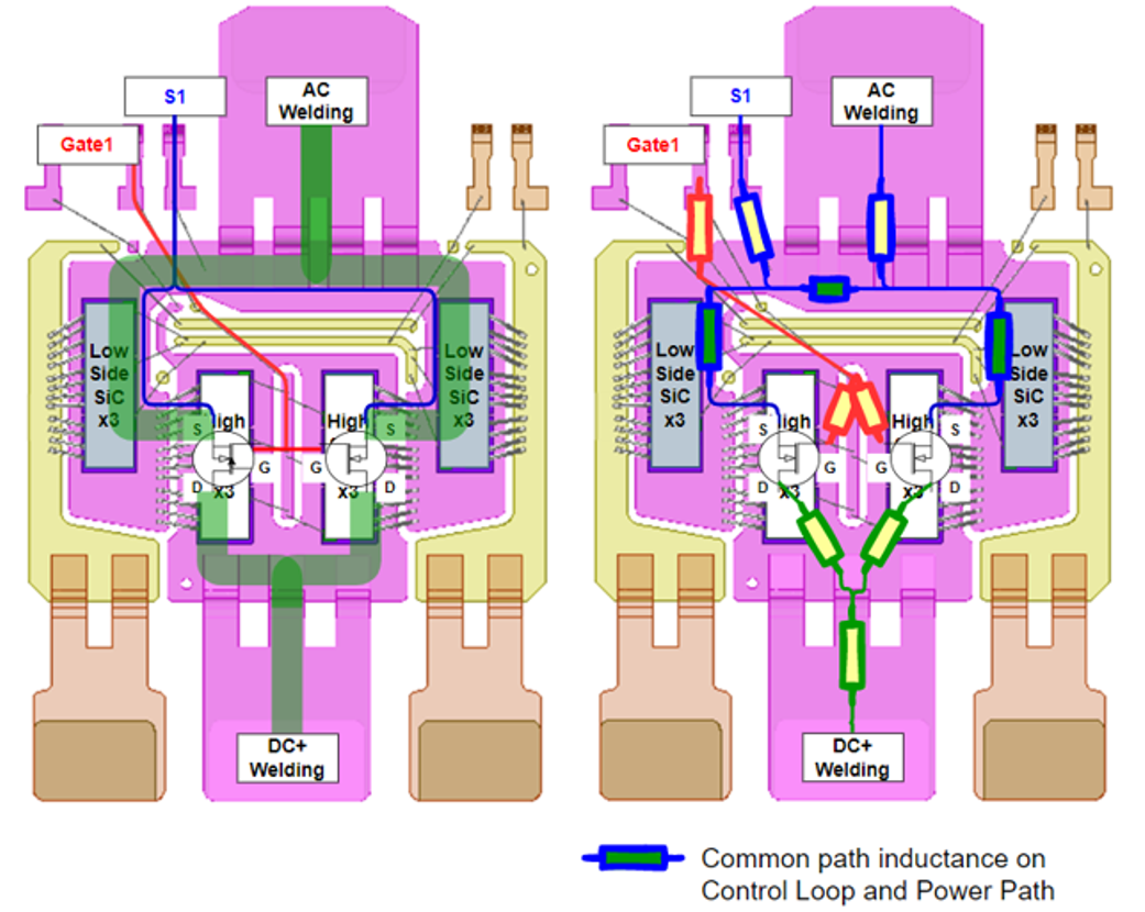
Fig.3 | Physical modeling maps the control-loop and power-path currents back onto the physical PCB layout segment by segment, highlighting the shared-path inductance where the two overlap.
The Culprit Revealed: High-Side Shared Inductance Is 2.9× the Low Side
The culprit soon revealed itself. When the control signal turns the SiC on and the current rises sharply, the shared-path inductance generates an induced voltage (Ls × di/dt) that suppresses the SiC’s gate voltage (VGS) from an ideal 14.5 V down to only about 5 V. With insufficient voltage, the SiC lingers in a “half-on” state of high on-resistance, prolonging the switching time and naturally sending energy loss soaring. Through segment-by-segment comparison with physical modeling, we calculated the high-side shared-path inductance at 6.07 nH—2.9× the low side’s 2.07 nH. This precisely explains why the high-side loss was so severe, and it maps exactly to the physical location on the PCB that needed correction.
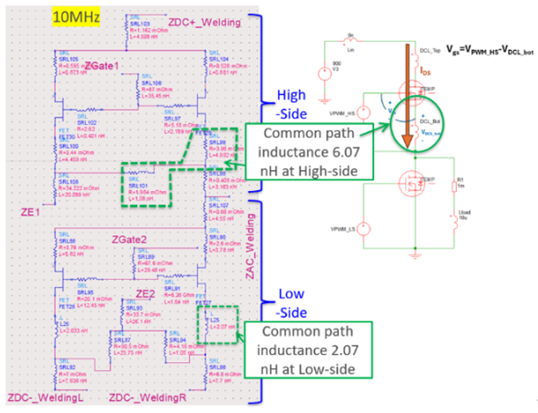
Fig.4 | The physical equivalent model quantifies the shared inductance at 6.07 nH on the high side versus 2.07 nH on the low side—a 2.9× gap—traceable to the physical location on the layout.
A Two-Pronged Solution: From “Design Rules” to the “Kelvin Connection”
Having found the culprit, USI proposed a two-pronged solution. In the short term, we fed the inductance values computed from physical modeling back into the simulation software to set an “upper limit” for the shared-path inductance, forming a reusable design rule that keeps future designs from repeating the same mistake. In the long term, we adopted a “Kelvin connection” design that fully separates the control loop from the power loop at the die pad, eliminating the shared path at its root. Although it calls for a few extra bonding wires, it significantly reduces switching loss while suppressing voltage ringing and preventing overshoot from exceeding specification and damaging the device. This was the solution ultimately adopted for the project.
Not Just a Manufacturer, but a JDM Partner
For USI, the value of this project lies in far more than solving a single technical problem. We established a standardized analysis flow that is “locatable, quantifiable, and reproducible”: layout flaws can be uncovered in advance at the simulation stage, compressing what used to take multiple rounds of trial and error into a single, right-first-time pass; and it lets us map out the “physical limits” of a customer’s design architecture, serving as the basis for deciding whether a major design change is warranted. Amid the accelerating adoption of EVs and SiC, USI is not merely a manufacturing partner, through its joint-design (JDM) role, it helps customers get efficiency, reliability, and manufacturability right from the very front end of design. This is precisely the core value we continue to deepen within the high-end power-module supply chain.
Looking ahead, SiC penetration across electric vehicles, energy storage, and industrial power will only keep climbing, and as power density is pushed ever higher, the impact of layout parasitics will be magnified further. This means that intercepting problems at the very front end of design will shift from a “nice-to-have” to a “must-have.” USI will continue extending this physical-modeling methodology to more high-end power-module and advanced-packaging projects and, combined with our long-accumulated expertise in System-in-Package (SiP) and advanced manufacturing, will offer customers an end-to-end service from design and simulation through to mass production. For supply-chain partners and investors alike, this represents a reliable collaborator capable of steadily turning cutting-edge technology into mass-producible products.
FAQ
Q1. What is a power module, and what role does it play in an EV?
A power module is an electronic module that integrates multiple power semiconductors (such as MOSFETs, IGBTs, and SiC). It is the core of an EV’s traction inverter, converting the battery’s DC into the AC that drives the motor. Its efficiency directly affects an EV’s range and performance.
Q2. Why are SiC power modules more susceptible to the PCB layout?
SiC switches much faster than a conventional IGBT, with a higher rate of current change (di/dt), making it more sensitive to the parasitic inductance introduced by the PCB layout. Even a tiny shared-path inductance can create an extra induced voltage that suppresses the gate voltage, drives up switching loss, and may even trigger voltage ringing.
Q3. What is “physical modeling,” and how does it differ from conventional numerical simulation?
Physical modeling builds an equivalent circuit according to the PCB’s actual current paths, so that every parasitic inductance and resistance maps to a specific location on the layout. Whereas numerical simulation can only show the “result” but struggles to localize the problem, physical modeling can point directly to “which path segment” is the source. This approach originates from the analytical thinking of RF engineering.
Q4. What was the most critical finding of this project?
Through physical modeling, USI found that the high-side shared-path inductance reached 6.07 nH—2.9× the low side’s 2.07 nH. This was the root cause of the nearly doubled high-side switching loss, and it could be mapped precisely to the physical location on the PCB layout.
Q5. What is a Kelvin connection, and why does it improve switching loss?
A Kelvin connection is a design that separates the control loop from the power loop at the die pad, completely eliminating their shared path and the associated parasitic inductance (Ls). Although it requires additional bonding wires, it significantly reduces switching loss and suppresses voltage ringing and overshoot, improving module reliability.
Q6. What role did USI play in this project?
This was USI’s first power-module JDM (Joint Design and Manufacturing) project. USI did more than manufacture: acting as a co-design partner, it helped the customer localize the problem at the earliest design stage, establish design rules, and propose solutions such as the Kelvin connection, working together with the customer to meet the performance targets.
Q7. What practical benefits does physical modeling bring to customers?
It can uncover layout flaws in advance at the simulation stage, compressing multiple rounds of trial and error into a single right-first-time pass and shortening development time. It also establishes reusable design rules that keep future designs from repeating mistakes, and it maps out the physical limits of the design architecture as a basis for deciding whether a major design change is warranted.
Search
Recent Articles
-
When AI Learns to “Read”: Using Deep Learning to Tame the False-Alarm Storm on SMT Production Lines
 When AI Learns to “Read”: Using Deep Learning to Tame the False-Alarm Storm on SMT Production Lines
07/13/2026
When AI Learns to “Read”: Using Deep Learning to Tame the False-Alarm Storm on SMT Production Lines
07/13/2026
-
Catching Invisible “Micro-Failures”: Safeguarding SiP Reliability Testing with Daisy Chains
 Catching Invisible “Micro-Failures”: Safeguarding SiP Reliability Testing with Daisy Chains
06/29/2026
Catching Invisible “Micro-Failures”: Safeguarding SiP Reliability Testing with Daisy Chains
06/29/2026
-
The Hidden Rival Inside an EV’s Heart: Cracking the Power-Loss Puzzle with “Physical Modeling”
 The Hidden Rival Inside an EV’s Heart: Cracking the Power-Loss Puzzle with “Physical Modeling”
06/17/2026
The Hidden Rival Inside an EV’s Heart: Cracking the Power-Loss Puzzle with “Physical Modeling”
06/17/2026
-
Behind the MFG. | From "Manufacturing" to "Creation" Ep.2: Innovation Built from Zero to One
 Behind the MFG. | From "Manufacturing" to "Creation" Ep.2: Innovation Built from Zero to One
05/28/2026
Behind the MFG. | From "Manufacturing" to "Creation" Ep.2: Innovation Built from Zero to One
05/28/2026
-
Behind the MFG. | From "Manufacturing" to "Creation" Ep.1: Unveiling USI’s Technological Vanguard
 Behind the MFG. | From "Manufacturing" to "Creation" Ep.1: Unveiling USI’s Technological Vanguard
05/07/2026
Behind the MFG. | From "Manufacturing" to "Creation" Ep.1: Unveiling USI’s Technological Vanguard
05/07/2026
-
Breaking the AI Energy Wall: Power Block and 3D Miniaturization Solutions
 Breaking the AI Energy Wall: Power Block and 3D Miniaturization Solutions
12/31/2025
Breaking the AI Energy Wall: Power Block and 3D Miniaturization Solutions
12/31/2025
-
Mastering Automotive HPC: Defining the "Sweet Spot" of SoMoG Technology
 Mastering Automotive HPC: Defining the "Sweet Spot" of SoMoG Technology
12/15/2025
Mastering Automotive HPC: Defining the "Sweet Spot" of SoMoG Technology
12/15/2025
-
【Smart Power Supply】Innovative Solution for DAC Control Bias Current
 【Smart Power Supply】Innovative Solution for DAC Control Bias Current
10/21/2025
【Smart Power Supply】Innovative Solution for DAC Control Bias Current
10/21/2025
-
From Experience to Precision: How AI Algorithms Enable Efficient RF Prediction Models
 From Experience to Precision: How AI Algorithms Enable Efficient RF Prediction Models
09/11/2025
From Experience to Precision: How AI Algorithms Enable Efficient RF Prediction Models
09/11/2025
-
Event|DIGITIMES 2025 D Forum – USI Shares How Heterogeneous Integration Drives a New Landscape for MCU Applications
 Event|DIGITIMES 2025 D Forum – USI Shares How Heterogeneous Integration Drives a New Landscape for MCU Applications
08/15/2025
Event|DIGITIMES 2025 D Forum – USI Shares How Heterogeneous Integration Drives a New Landscape for MCU Applications
08/15/2025
Keep up with top trending topic
For the latest innovation technology, application
and industry insight.
Subscribe Our Blog
For the latest innovation technology, application
and industry insight.