
USI Blog
Top trending topic for the latest innovation technology, application and industry insight.
Search
- 06/29/2026
Catching Invisible “Micro-Failures”: Safeguarding SiP Reliability Testing with Daisy Chains

Author:Emily Fei/AMMS / MWC Hardware Design Engineer
When a System-in-Package (SiP) crams the processor, memory, and RF module into a space the size of a fingernail, what worries engineers most is often not “whether it works,” but whether those solder joints, which are finer than a strand of hair, can survive after a phone is dropped on the ground, after automotive electronics run at high temperatures beside the engine, or after a product is repeatedly subjected to heat and vibration during shipping.
As electronic products evolve toward higher performance, miniaturization, and multifunctionality, SiP, with its high integration and packaging flexibility, has been widely adopted in consumer electronics, communications, and automotive electronics. Yet precisely because of its complex structure and diverse materials, the coupling effects of thermal, electrical, and mechanical stress are especially pronounced, making board-level reliability the gate that customers care about most. The answer to that gate is the Board Level Reliability Test (BLRT).
BLRT is a type of interconnect reliability test, covering items such as bending, shock, vibration, temperature cycling, and high temperature/high humidity. It has three objectives: to verify the reliability of solder-joint interconnections at every level, to ensure the robustness of IC and module packaging, and to validate whether an IC, once assembled onto a circuit board, can withstand mechanical and environmental stress. USI’s R&D team uses an ingenious design to “rehearse” these real-world ordeals: the Daisy Chain test structure.
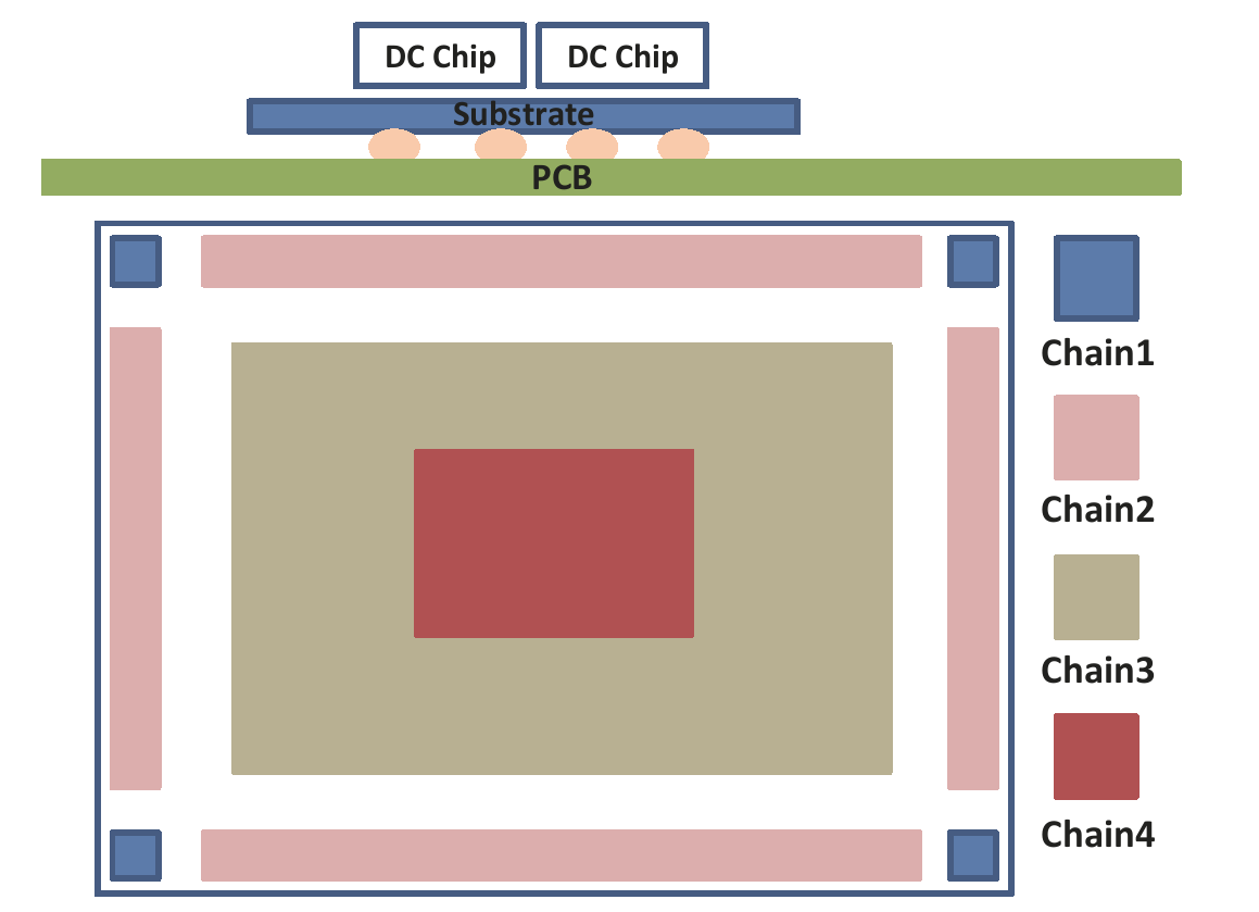
Fig1. Daisy Chain Structure
Stringing “Dummy Dies” into a Circuit That Talks
At the heart of the daisy chain test is a group of “daisy chain dies” that are deliberately stripped of any function. Identical in appearance to real dies, they connect first through the first-level solder joints to the module substrate, then through the second-level solder joints to the test board (EVB PCB), and finally to external test points, stringing every solder ball inside the entire package into one complete, closed circuit loop.
The beauty of this design is that the moment a solder joint cracks or fractures during testing, the loop’s resistance immediately jumps. In other words, a microscopic failure invisible to the naked eye is translated into a measurable electrical signal. Notably, daisy chain designs are graded into three levels, and only Level 3 is considered qualified: it must fully cover the silicon die’s metal layer, the redistribution layer (RDL), and the bumps/solder balls. That means BLRT monitors not only the “die-to-board” soldering, but also the RDL, bumps, and even cracks in the silicon die itself, none of which can escape its eye.
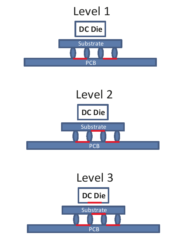
Figure 2. Daisy Chain Design Levels
Four Chains, Each Responsible for Its Own “Torture Test”
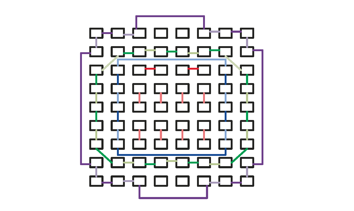
Fig3. Four Chains Package Pins Arrangement Example
USI’s daisy chain design divides the entire module into four independent loops, each corresponding to a different stress test, so that problems can be pinpointed precisely:
- Chain 1 (Package Core / CSP): Connected to the IC die; mainly inspects UBM pad strength and the solderability between the die and the module pads.
- Chain 2 (Module Edge): Inspects the connection between the outermost solder balls of the module and the EVB PCB, corresponding to the mechanical Shock test.
- Chain 3 (Module Center): Inspects the connection between the central-area solder balls and the PCB, corresponding to the Temperature Cycling and High-Temperature/High-Humidity (TCT / THD) tests.
- Chain 4 (Four Corners): Inspects the connection between the four corners and the PCB, corresponding to the Bend test.
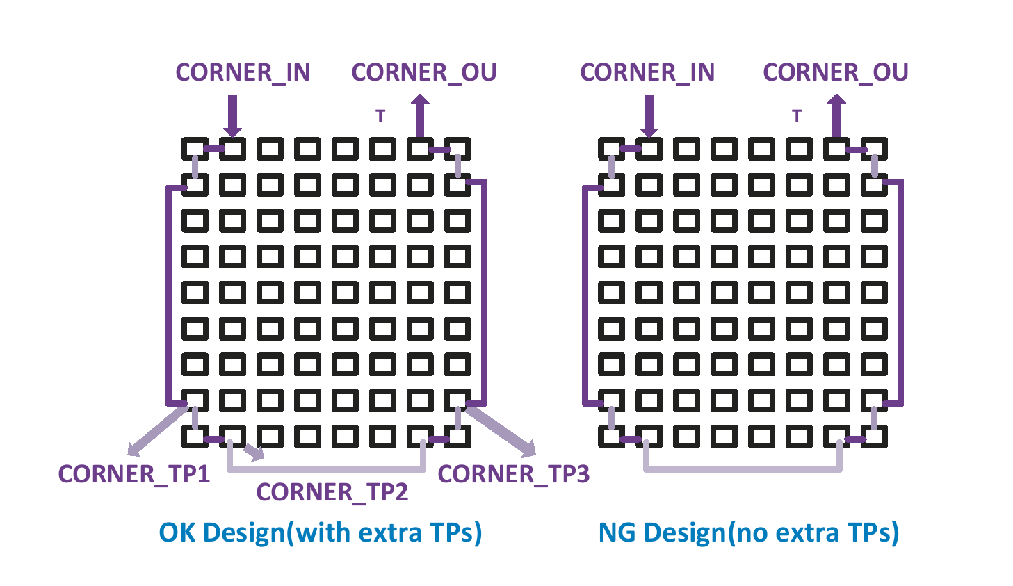
Fig4. Corner balls array rules
Making the “Test Sample” Mirror the “Mass-Production Part”
For BLRT to be meaningful, the daisy chain module must reproduce, as closely as possible, the real behavior of the mass-production functional module. There are quite a few design “knacks” involved here. First is the copper rate: in principle, the difference in copper content of each layer between the daisy chain module and the functional module should be kept within 15%, so that their thermal and mechanical stress responses match. The bottom layer, however, is especially tricky—the functional module’s bottom layer has numerous ground pads that can be spread into a large ground plane, whereas the daisy chain module has no ground pins and every ball is a node. Differences in the bottom layer therefore often require negotiation and approval with the customer.
Next is routing and layout: experience shows that routing traces on inner layers rather than the surface layer reduces the stress they bear; on inner layers, via sizes should be enlarged and trace widths widened as much as possible to mitigate environmental stress. Corners and pad junctions adopt a teardrop design to avoid abrupt changes in trace width that cause signal reflection and fracture, giving a smooth transition from the trace to the component pad.
Finally, the EVB pads: pads come in two types: SMD (Solder Mask Defined, where solder mask covers the pad copper) and NSMD (Non-Solder Mask Defined, i.e., metal-defined). Based on USI’s testing experience from past WiFi projects, the SMD design is more favorable for the subsequent underfill dispensing and improves the overall robustness of the solder joints under board-level reliability testing. In addition, the termination pairs and GND pins in the package design must also be correspondingly connected on the test PCB to fully close the loop.
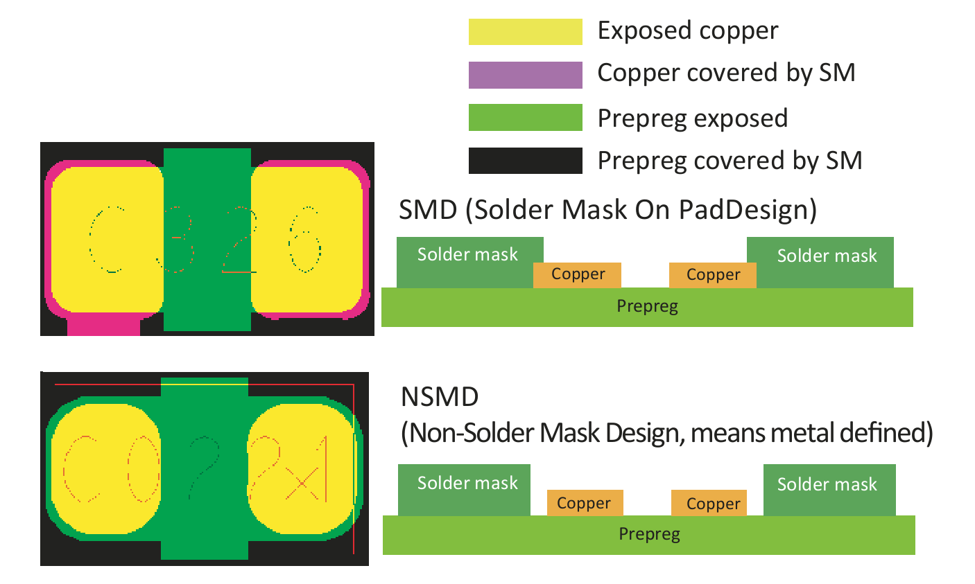
Fig5. Solder Mask Definition Comparison
Precise Data Behind the Validation System
In the past, board-level reliability validation relied largely on manual operation and fragmented management: the process depended on experience and lacked standardization, tests were lengthy, equipment occupancy was high, and human error was common. Failure analysis could often only be inferred by disassembling a sample after it had failed, time-consuming, insufficiently precise, and difficult to use for preventing problems in advance.
Now, USI’s R&D team has thoroughly upgraded the entire process. Building on international standards such as JEDEC and IPC and incorporating customers’ specific requirements, we have established a standardized test flow covering temperature cycling, thermal shock, high temperature/high humidity, mechanical shock, and drop. Before testing, we use Finite Element Analysis (FEA) and thermal-mechanical simulation to predict high-risk solder joints and optimize sample design; during testing, we deploy automated equipment and real-time data acquisition, complemented by big-data trend analysis to rapidly catch anomalies; and when failures occur, we apply advanced techniques such as X-Ray, C-SAM, FIB, and SEM, together with solder-joint fatigue life models, to precisely locate the failure mechanism. The three are tightly interlocked, transforming reliability validation from “leaving it to luck” into “being in control.” The concrete results of this effort are remarkable, including:
- The overall test cycle was shortened by about 50%, meeting customers’ need for fast validation.
- Failure-analysis accuracy was raised to over 90%, with more complete reports and more targeted improvement recommendations, reducing repeated validation.
- A digitalized project platform lets customers view progress and reports in real time, improving communication efficiency by about 70%.
- Process standardization and automation, together with simulation that lowers the failure rate, reduced overall project cost by about 20%.
- A replicable validation system and technical templates were accumulated, ready for rapid deployment in subsequent SiP projects.
A Commitment From “Teardown” to “Prediction”
For customers, daisy chain BLRT is not merely a test report but a certificate of trust attesting that “this SiP can withstand the trials of shipping, assembly, and long-term use.” USI’s R&D team integrates standardized processes, simulation-based prediction, and advanced failure analysis into a replicable, traceable validation system, enabling every new SiP project to be rapidly deployed and stably mass-produced.
In the advanced packaging supply chain, we serve not only as a manufacturer but as a reliability partner that safeguards quality and lifespan for customers in advance. By turning “invisible reliability” into “visible data” through scientifically rigorous design and validation, USI is able to keep winning customers’ trust in the era of System-in-Package—and that is the key.
Frequently Asked Questions (Q&A)
Q1. What is SiP Board Level Reliability Testing (BLRT)?
A: BLRT is an interconnect reliability test performed after a System-in-Package (SiP) has been assembled onto a circuit board, covering items such as bending, shock, vibration, temperature cycling, and high temperature/high humidity. Its three main objectives are to verify the reliability of solder-joint interconnections at every level, to ensure the robustness of IC and module packaging, and to validate whether an IC, once assembled onto the PCB, can withstand mechanical and environmental stress—thereby simulating the stress conditions a product may encounter during shipping, assembly, and use.
Q2. What role does the Daisy Chain design play in reliability testing?
A: The daisy chain design uses non-functional daisy chain dies to string all the solder balls inside the package into a closed circuit via the first- and second-level solder joints. When any solder joint cracks or fractures, the loop resistance changes, converting microscopic failures invisible to the naked eye into measurable electrical signals. It is the core method for monitoring SiP solder-joint reliability.
Q3. Why must the daisy chain design reach Level 3?
A: Daisy chain designs are graded into three levels, and only Level 3 is qualified. Level 3 is a continuous daisy chain that must fully cover the silicon die’s metal layer, the redistribution layer (RDL), and the bumps/solder balls. As a result, BLRT can validate not only the device-to-board solder joints but also failure modes such as cracks in the RDL and in the silicon die/bumps.
Q4. Why is the SMD design recommended for EVB pads?
A: EVB pads come in two types: SMD (Solder Mask Defined, where solder mask covers the pad copper) and NSMD (Non-Solder Mask Defined, i.e., metal-defined). Based on USI’s testing experience from past WiFi projects, the SMD design is more favorable for the subsequent underfill dispensing and improves the overall robustness of solder joints under board-level reliability testing.
Q5. What technical advantages and results does USI have in SiP board-level reliability testing?
A: USI builds standardized processes by combining JEDEC and IPC standards with customer requirements, uses Finite Element Analysis (FEA) and thermal-mechanical simulation for up-front failure prediction, deploys automated testing and real-time data acquisition, and applies advanced failure-analysis techniques such as X-Ray, C-SAM, FIB, and SEM. Tangible results include shortening the test cycle by about 50%, raising failure-analysis accuracy to over 90%, improving communication efficiency by about 70%, and lowering overall cost by about 20%.
Q6. What is the practical value of board-level reliability testing for SiP customers?
A: For customers, a complete BLRT is a certificate of trust that “the product can withstand the trials of shipping, assembly, and long-term use.” USI integrates standardized processes, simulation-based prediction, and failure analysis into a replicable, traceable validation system, helping customers accelerate design optimization, reduce repeated validation, and achieve smooth mass production. It serves as a reliability partner in the advanced packaging supply chain that safeguards quality and lifespan for customers in advance.
Search
Recent Articles
-
When AI Learns to “Read”: Using Deep Learning to Tame the False-Alarm Storm on SMT Production Lines
 When AI Learns to “Read”: Using Deep Learning to Tame the False-Alarm Storm on SMT Production Lines
07/13/2026
When AI Learns to “Read”: Using Deep Learning to Tame the False-Alarm Storm on SMT Production Lines
07/13/2026
-
Catching Invisible “Micro-Failures”: Safeguarding SiP Reliability Testing with Daisy Chains
 Catching Invisible “Micro-Failures”: Safeguarding SiP Reliability Testing with Daisy Chains
06/29/2026
Catching Invisible “Micro-Failures”: Safeguarding SiP Reliability Testing with Daisy Chains
06/29/2026
-
The Hidden Rival Inside an EV’s Heart: Cracking the Power-Loss Puzzle with “Physical Modeling”
 The Hidden Rival Inside an EV’s Heart: Cracking the Power-Loss Puzzle with “Physical Modeling”
06/17/2026
The Hidden Rival Inside an EV’s Heart: Cracking the Power-Loss Puzzle with “Physical Modeling”
06/17/2026
-
Behind the MFG. | From "Manufacturing" to "Creation" Ep.2: Innovation Built from Zero to One
 Behind the MFG. | From "Manufacturing" to "Creation" Ep.2: Innovation Built from Zero to One
05/28/2026
Behind the MFG. | From "Manufacturing" to "Creation" Ep.2: Innovation Built from Zero to One
05/28/2026
-
Behind the MFG. | From "Manufacturing" to "Creation" Ep.1: Unveiling USI’s Technological Vanguard
 Behind the MFG. | From "Manufacturing" to "Creation" Ep.1: Unveiling USI’s Technological Vanguard
05/07/2026
Behind the MFG. | From "Manufacturing" to "Creation" Ep.1: Unveiling USI’s Technological Vanguard
05/07/2026
-
Breaking the AI Energy Wall: Power Block and 3D Miniaturization Solutions
 Breaking the AI Energy Wall: Power Block and 3D Miniaturization Solutions
12/31/2025
Breaking the AI Energy Wall: Power Block and 3D Miniaturization Solutions
12/31/2025
-
Mastering Automotive HPC: Defining the "Sweet Spot" of SoMoG Technology
 Mastering Automotive HPC: Defining the "Sweet Spot" of SoMoG Technology
12/15/2025
Mastering Automotive HPC: Defining the "Sweet Spot" of SoMoG Technology
12/15/2025
-
【Smart Power Supply】Innovative Solution for DAC Control Bias Current
 【Smart Power Supply】Innovative Solution for DAC Control Bias Current
10/21/2025
【Smart Power Supply】Innovative Solution for DAC Control Bias Current
10/21/2025
-
From Experience to Precision: How AI Algorithms Enable Efficient RF Prediction Models
 From Experience to Precision: How AI Algorithms Enable Efficient RF Prediction Models
09/11/2025
From Experience to Precision: How AI Algorithms Enable Efficient RF Prediction Models
09/11/2025
-
Event|DIGITIMES 2025 D Forum – USI Shares How Heterogeneous Integration Drives a New Landscape for MCU Applications
 Event|DIGITIMES 2025 D Forum – USI Shares How Heterogeneous Integration Drives a New Landscape for MCU Applications
08/15/2025
Event|DIGITIMES 2025 D Forum – USI Shares How Heterogeneous Integration Drives a New Landscape for MCU Applications
08/15/2025
Keep up with top trending topic
For the latest innovation technology, application
and industry insight.
Subscribe Our Blog
For the latest innovation technology, application
and industry insight.