Search
- 11/14/2024
Front-End Design System (FEDS): A Hundredfold Efficiency Revolution for PCB Layout Review Automation!
In traditional PCB development processes, to meet tight development schedules, we often find that layout engineers and various functional development teams are required to resolve all violations in inspection reports within a week. For a single CPU, the number of violations in an inspection report is around three to four thousand, and for a dual CPU, it often reaches seven to eight thousand.
This requirement implies that hardware and power development engineers need to review and modify designs in real-time. Additionally, it requires four to five layout engineers to work overtime daily to manually correct all violations.
Four Pain Points in Traditional PCB Review Processes
Under extreme time constraints, improving efficiency and increasing processing time becomes the primary goal. Therefore, the CE R&D team at USI has identified four key pain points from accumulated development projects, with the first one being the most critical:
- How to improve the efficiency of correcting layout violations and accelerate the process of entering Gerber output for production?
- How to integrate inspection requirements from different sources to reduce the burden of engineers?
- How to unify inspection standards for various functions to avoid differences in human standards?
- How to memorize various inspection items and regulations to reduce the workload of engineers for each inspection?
Solutions - What is a Front-End Design System (FEDS)?
A Front-End Design and Simulation Automation Platform (FEDS) is a proprietary tool developed by USI to enhance the efficiency and quality of electronic product design. At its core, FEDS automates many repetitive and error-prone tasks in the design process. From initial bill of materials (BOM) generation and verification to subsequent schematic and PCB layout inspections, and even complex electromagnetic simulations, FEDS provides comprehensive automated support. This significantly reduces product development cycles and minimizes human error.
Think of FEDS as a Google platform specifically designed for electronic design. Beyond circuit layout review, it offers a wide range of tools including: BOM generation and verification, Schematic checks, Simulation of electrical characteristics (RF, PI simulation) to ensure compliance with electrical specifications, Online collaborative RF matching including RF characteristic optimization, RF test automation, and comparison of RF simulation results.
The greatest differentiator of the FEDS automation platform is its extreme flexibility for customization. Traditional commercial EDA tools often have overly generic functionalities, while FEDS allows companies to develop and integrate their own inspection rules and simulation tools based on their specific product characteristics and design processes. This enables FEDS to more accurately meet the needs of enterprises and improve design efficiency.
PCB Layout Review Automation
PCB development engineers have four primary needs when conducting PCB layout reviews:
- Third-party tools commonly used to verify that CPU signal interfaces comply with their specifications.
- Design guidelines (PDGs) from various platforms that specify requirements for different signal interfaces.
- Design experience and requirements from various R&D units and manufacturing departments within the company.
- Specific inspection requirements from customer R&D engineers for the product.
Currently, there are five main categories of automated PCB layout review tools, including Routing Check, Pad and Placement Check, and Via Check. Furthermore, automated PCB layout review can develop proprietary inspection items tailored to specific product needs, such as:
- Differential signal trace symmetry check: Ensures that differential signals have symmetrical traces at the pad and via exit points.
- Cross-talk prevention check: Ensures that differential signal pads and vias are not crossed by other signals to minimize interference.
- Ground via density check: This function allows layout engineers to quickly inspect the power distribution network (PDN) upon initial completion of routing, addressing power integrity issues early on and significantly saving time and resources.
Results

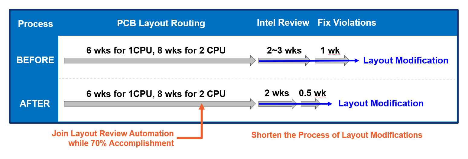
Figure 1. Comparison of PCB Layout development time optimization through automated review tools
Automated PCB layout review tools can automatically identify and correct violations before 70% of the routing is completed in the schematic. In the overall development process, two significant optimizations have been observed:
1. Accuracy and consistency in finding violations on board files
o Before implementation: Relied on experienced engineers, with inconsistent opinions, resulting in low efficiency and time consumption.
o After implementation: Automated inspection with unified standards, reducing the total time for checking and correcting violations.
2. Comparison of efficiency between automated and manual inspection
o Before implementation: Manual inspection was time-consuming, especially for large-scale projects.
o After implementation: Automated inspection is fast, significantly improving efficiency and reducing the need for repetitive tasks by engineers.
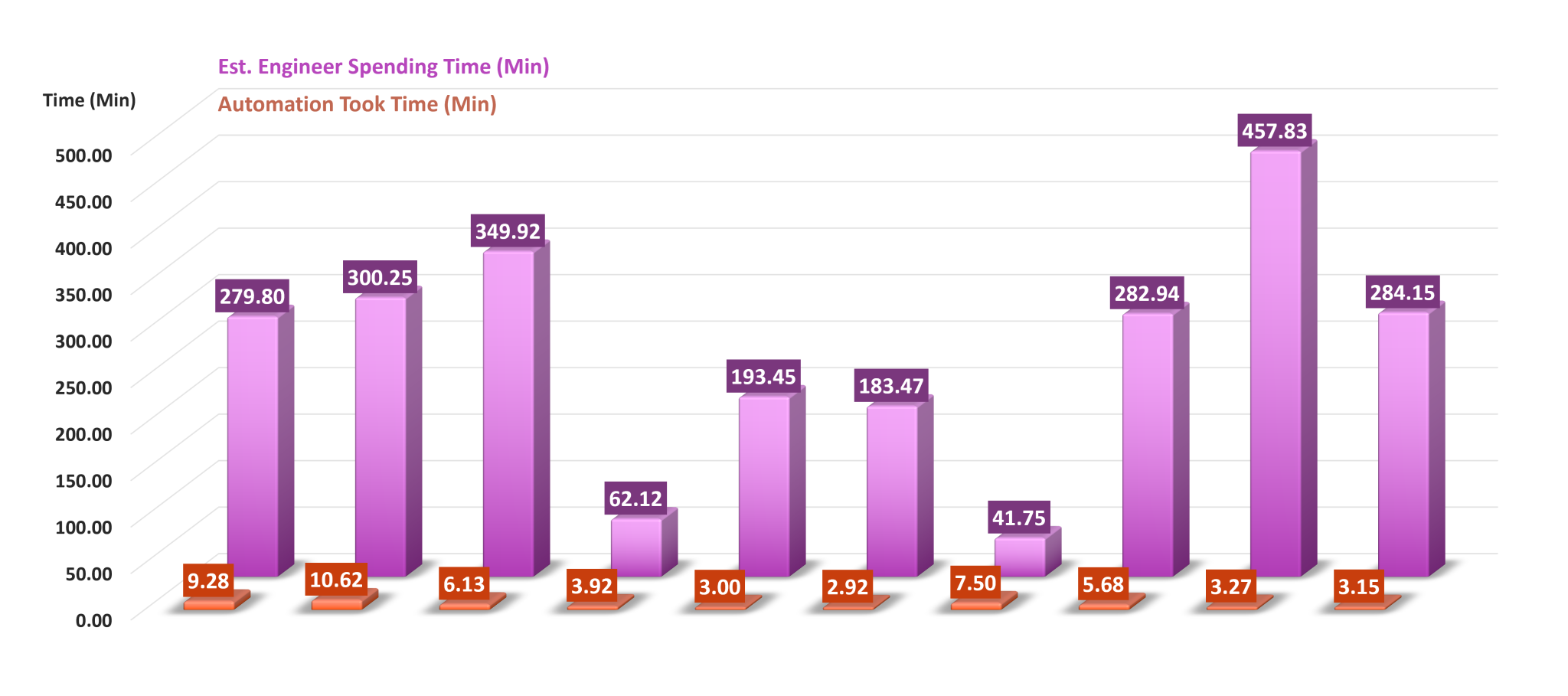
By analyzing the layout projects in 2023 and comparing the working hours of automated and manual inspections, Figure 2 clearly shows a difference of more than ten times, or even hundreds of times. This demonstrates the significant contribution of automation to improving layout review efficiency.

Figure 2. Comparison of working hours between manual and automated inspection
In conclusion, the introduction of an automated inspection system has brought multiple benefits to the enterprise:
- Significantly accelerates product development efficiency: Shortens layout inspection time and accelerates product time-to-market.
- Improves consistency and reliability of inspection results: Reduces errors caused by human factors.
- Flexibility of the automated platform: Can develop customized inspection items for different products and processes.
- Enhances product quality: Early detection and resolution of design issues reduce product defects.
Keep up with top trending topic
For the latest innovation technology, application
and industry insight.
Subscribe Our Blog
For the latest innovation technology, application
and industry insight.


