USI Blog
Top trending topic for the latest innovation technology, application and industry insight.
Search
- 05/18/2022
USI 5G RF Circuit Design and Validation: Optimizing Board Level Development Efficiency
After 4G evolved into 5G, broader bandwidths and new frequency bands have disrupted how testing will bedone. Mass production and testing for 5G production have become ever more challenging. According to researchers, billions of 5G devices will be on the market in the next few years. All the brand owners will need to deliver high quality products with limited budgets.
How to manage the cost within a limited range should be considered from the stage of product design. Moreover, accelerating time-to-market will also become a crucial point of the competition between enterprises.
Following the previous article, “USI Advanced 5G Turnkey Services & Two Challenges You Need to Overcome When Developing 5G Products,” this article continues the deep dive into the second stage in 5G RF development, board level design, and validation. This article will also discuss how simulating validation can help overcome the many hurdles of product development.
Learn More: USI Advanced 5G Turnkey Services & Two Challenges You Need to Overcome When Developing 5G Products
The Second Stage in 5G Development: Simulating and Validating Board level Design
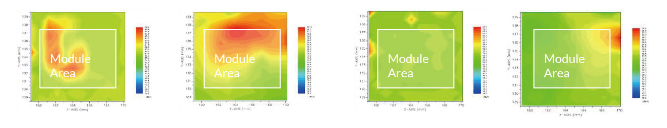
In the previous article, we have shown that 5G product development can be time-consuming due to iterations of design, simulation, and validation. With USI’s expertise in mainstream validation software and extensive experience in simulation and design, we can use simulation to generate data close to real model of products in early development stage. Only when antenna simulation and RF simulation meet or exceed 80% of customers’ specifications, would USI proceed to materialization validation with printed circuit boards.
In this stage, most EMS manufacturers will need to re-optimize or redesign their printed circuit boards due to a lack of pre-test simulation which leads to discrepancies with customer specifications. However, USI can afford to spend less time on optimization, since we do sufficient analysis and are able to verify design accuracy in early stages without needing to resort to incessant testing and adjusting. The development team can reach high accuracy in the stage of design simulation.
USI takes the design, production, and validation testing of
industrial level products more seriously than average products.
This has helped USI accumulate tremendous bodies of
professional knowledge, practical foundations, and manufacturing process experience.
Keys to Accelerate Time-to-Market: Integrating Design of Antennas, RF Circuit, and Mechanisms
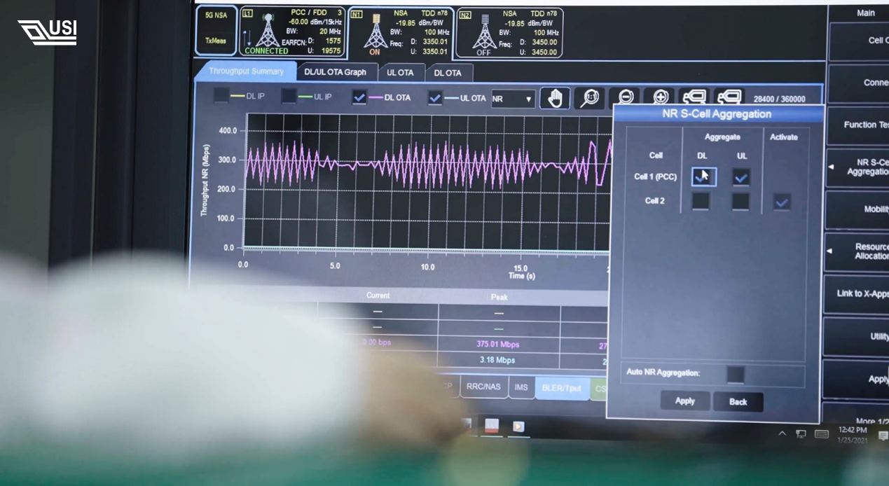
To proceed to system testing, each 5G products must overcome the challenges of design, simulation, and validation. This includes the designs of RF Circuit, antennas, and mechanisms. To meet the right specifications, USI first touches base with customers for product specifications, RF design structures, and product-related regulatory requirements. Next, in designing circuit diagrams and layouts, USI uses simulation to ensure the designs meet customer’s specifications as well as protocol requirements.
Each phase in design and verification can take more than two months, not to mention antenna, RF circuit, and mechanism systems cannot success alone. Any slightest negligence in the integration between the three parties may result in the off-gauge and need to be redesigned.
In the past, a customer attempted to develop 5G products on its own, but due to the lack of 5G development experience and appropriate simulation facilities, the customer only discovered before mass production that after the product was assembled, its radiator and mechanism design could not satisfy legal requirements. The customer had to start over after investing in all the budget and time. After seeking professional guidance, the customer consulted USI and successfully solved the product’s heating problem and met legal requirements. USI is well-known that each product has its idiosyncrasies by exploring various product lines to accumulate experience in design and manufacturing. Nowadays, USI’s versatile know-how can offer customers better solutions when facing different requirements.Through integrating the professional
capabilities and equipment needed in the three phases,
USI can help customers develop products
by vastly reduce communication time and miscommunication risk.
The Power of Miniaturization: Getting More in Less
As technology advances, tech products are gaining new functions gradually, which doubles their needs for components. Manufacturing processes are hence now trending towards miniaturizing process. When it comes to Board level designs, space is the key to the overall design. Miniaturization techniques are thus crucial. For example, how to downsize the space of RF components need without affecting the overall performance and free up space for antenna layout?
When space is limited, products tend to have
impedance mismatches or mutual interference in RF circuit.
However, through System-in-Packing manufacturing technologies,
30 to 40% space may be saved for other designs.
Apart from design and validation capabilities, through miniaturization design and the system-in-package (SiP) technology, the antenna can be downsized even more in the future, enhancing the efficiency of other components, and providing more design flexibility. Technically, smaller modules mean shorter signal paths, which help reduce stray capacitance and the Inductance effect to achieve higher signal integrity and transmission speed. At USI, we take a system integration approach to offer advanced 5G turnkey services to simplify product design and cut the development schedule and budget.
Read More: How to Develop Products with Miniaturization Techniques?
Providing Comprehensive Validation Equipment and Testing Environments by Advanced 5G Turnkey Services
Within the industry, most projects are initiated upon customer requests, after which specifications ensue, followed by layout and design. At this stage, due to the mutual influence between antennas, RF circuit, and mechanisms, developers often spend months to coordinate and adjust. Even so, the developed samples are still at risk for not meeting customer specifications, thus requiring another round of design. Such repetitive stages in development can be described as the developmental barriers between 4G and 5G. Countless hours of human resources can be spent in this process, accounting for most of the costs for brand customers.
By integrating antenna, RF circuit, and mechanism team into a comprehensive 5G turnkey services, USI vastly reduces the coordinating needs for customers, which often accompanies extensive communication time and risk for miscommunication. Through providing accurate simulations for Board level design and rigorous but efficient validation services, USI avoids the conventional repetitive process of optimizing, redesigning, and revalidating, preventing customers from spending time in repetitive processes, shortening project development schedule and lowering project costs. This is one of USI’s most valuable services it offers to customers.
In order to prepare for the future market of a billion 5G devices, brand customers need to collaborate with trustworthy partners in 5G development and manufacturing to overcome development barriers and deliver high-quality products to breakthrough to gain an upper-hand in the competitive 5G market.
Search
Recent Articles
-
Catching Invisible “Micro-Failures”: Safeguarding SiP Reliability Testing with Daisy Chains
 Catching Invisible “Micro-Failures”: Safeguarding SiP Reliability Testing with Daisy Chains
06/29/2026
Catching Invisible “Micro-Failures”: Safeguarding SiP Reliability Testing with Daisy Chains
06/29/2026
-
The Hidden Rival Inside an EV’s Heart: Cracking the Power-Loss Puzzle with “Physical Modeling”
 The Hidden Rival Inside an EV’s Heart: Cracking the Power-Loss Puzzle with “Physical Modeling”
06/17/2026
The Hidden Rival Inside an EV’s Heart: Cracking the Power-Loss Puzzle with “Physical Modeling”
06/17/2026
-
Behind the MFG. | From "Manufacturing" to "Creation" Ep.2: Innovation Built from Zero to One
 Behind the MFG. | From "Manufacturing" to "Creation" Ep.2: Innovation Built from Zero to One
05/28/2026
Behind the MFG. | From "Manufacturing" to "Creation" Ep.2: Innovation Built from Zero to One
05/28/2026
-
Behind the MFG. | From "Manufacturing" to "Creation" Ep.1: Unveiling USI’s Technological Vanguard
 Behind the MFG. | From "Manufacturing" to "Creation" Ep.1: Unveiling USI’s Technological Vanguard
05/07/2026
Behind the MFG. | From "Manufacturing" to "Creation" Ep.1: Unveiling USI’s Technological Vanguard
05/07/2026
-
Breaking the AI Energy Wall: Power Block and 3D Miniaturization Solutions
 Breaking the AI Energy Wall: Power Block and 3D Miniaturization Solutions
12/31/2025
Breaking the AI Energy Wall: Power Block and 3D Miniaturization Solutions
12/31/2025
-
Mastering Automotive HPC: Defining the "Sweet Spot" of SoMoG Technology
 Mastering Automotive HPC: Defining the "Sweet Spot" of SoMoG Technology
12/15/2025
Mastering Automotive HPC: Defining the "Sweet Spot" of SoMoG Technology
12/15/2025
-
【Smart Power Supply】Innovative Solution for DAC Control Bias Current
 【Smart Power Supply】Innovative Solution for DAC Control Bias Current
10/21/2025
【Smart Power Supply】Innovative Solution for DAC Control Bias Current
10/21/2025
-
From Experience to Precision: How AI Algorithms Enable Efficient RF Prediction Models
 From Experience to Precision: How AI Algorithms Enable Efficient RF Prediction Models
09/11/2025
From Experience to Precision: How AI Algorithms Enable Efficient RF Prediction Models
09/11/2025
-
Event|DIGITIMES 2025 D Forum – USI Shares How Heterogeneous Integration Drives a New Landscape for MCU Applications
 Event|DIGITIMES 2025 D Forum – USI Shares How Heterogeneous Integration Drives a New Landscape for MCU Applications
08/15/2025
Event|DIGITIMES 2025 D Forum – USI Shares How Heterogeneous Integration Drives a New Landscape for MCU Applications
08/15/2025
-
Shielding Fence: SiP Technology at the Hair-thin level
 Shielding Fence: SiP Technology at the Hair-thin level
07/16/2025
Shielding Fence: SiP Technology at the Hair-thin level
07/16/2025
Keep up with top trending topic
For the latest innovation technology, application
and industry insight.
Subscribe Our Blog
For the latest innovation technology, application
and industry insight.