
USI Blog
Top trending topic for the latest innovation technology, application and industry insight.
Search
- 11/09/2026
Exposing Warpage Risk Inside the Reflow Oven: A 3D “Contour Map” at 260°C
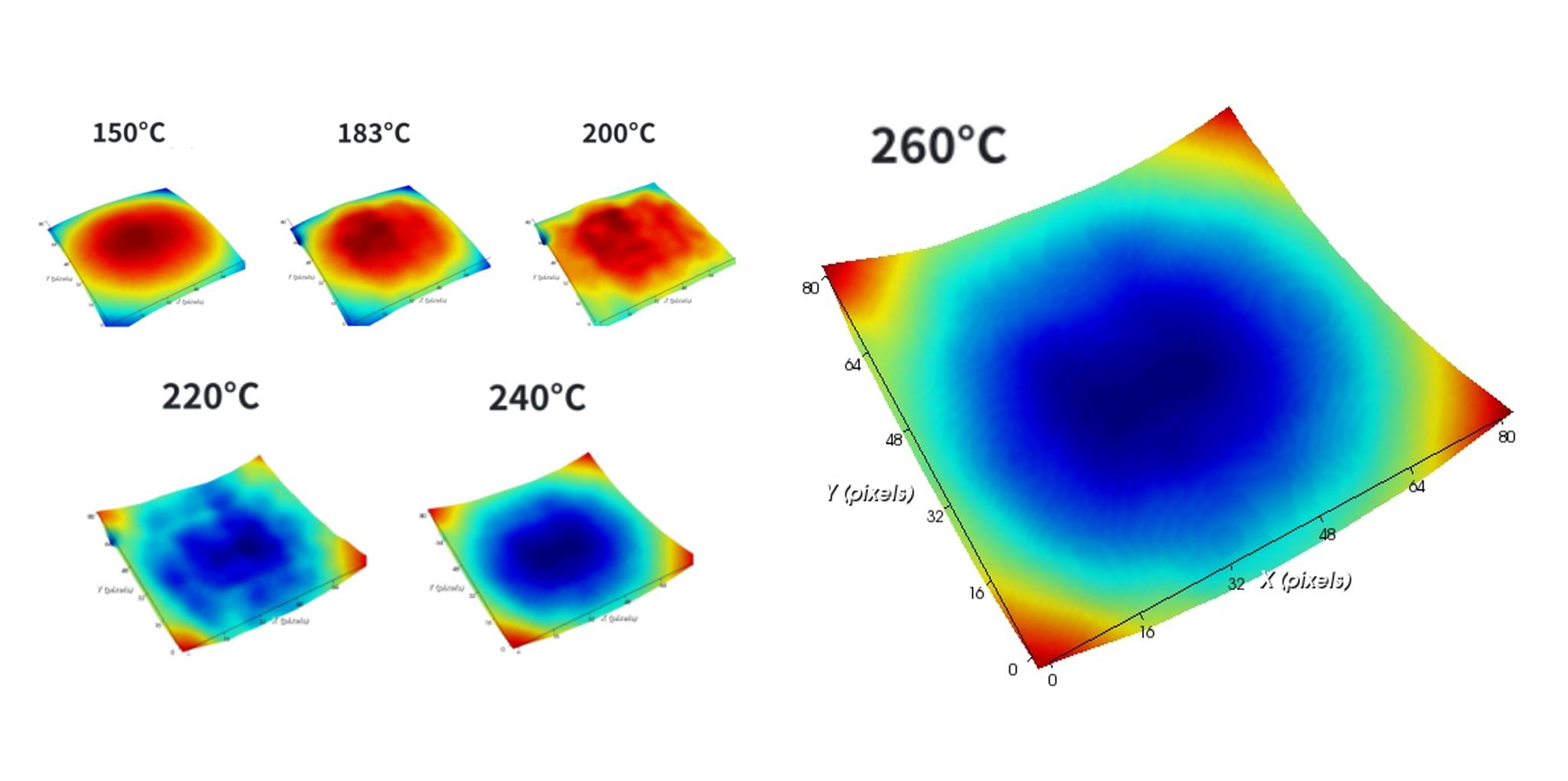
Author: Kevin Hong, Manager of Process Engineering (TW OPS/MSC)
An AI server motherboard can carry tens of thousands of solder balls, each less than 1 mm in diameter, that must melt and solidify together in a reflow oven at around 260°C to bond the chips firmly to the board. The catch: packages do not stay flat when heated. Like potato chips in an oven, they bend slightly.
During one new component introduction, we measured a 21 mm × 21 mm BGA package: at 260°C, its warpage reached 229 µm—just 1 µm below the 230 µm JEDEC limit. The component “passed,” but it was standing at the edge of a cliff. Had we followed conventional practice and applied standard stencil apertures based on ball pitch alone, the solder balls at the four corners would likely have been squashed and bridged into shorts. USI’s process team took a different route: before the first trial build, we used Shadow Moiré to see the warpage clearly, then translated the data into stencil aperture design.
Why Do Chips “Bend” in the Reflow Oven?
A BGA (Ball Grid Array) package places its interconnects as an array of solder balls across its underside. The package is a stack of materials—die, substrate, and molding compound—each with a different coefficient of thermal expansion (CTE). When heated, some expand more than others, and the whole package bends, much like the bimetallic strip in a thermometer.
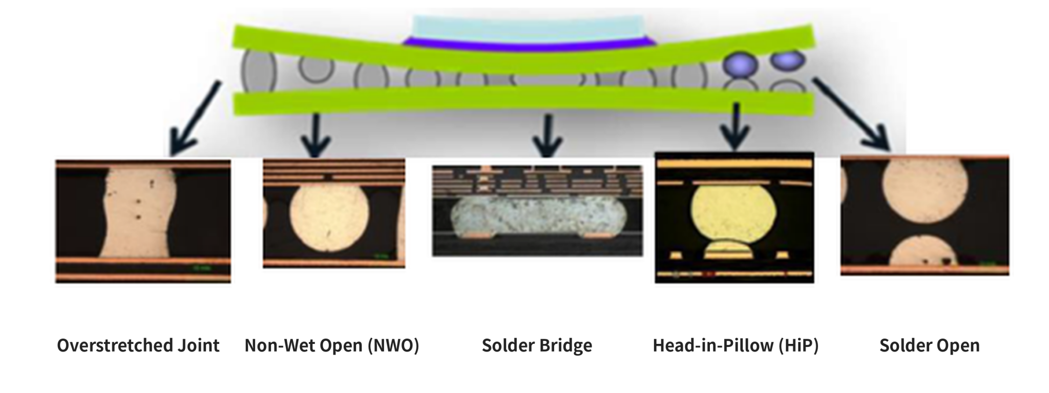
Figure 1: Five solder joint defects that BGA package warpage can cause (cross-section images)
Shadow Moiré: A 3D “Contour Map” of the Chip
Picture sunlight passing through window blinds: the shadows bend as they fall across an uneven wall. Shadow Moiré is a precision version of this principle. A grating ruled with fine parallel lines is placed above the sample and illuminated with white light at an angle. The grating and its shadow on the package surface overlap to form alternating light and dark moiré fringes. Each fringe acts like a contour line; a camera captures the pattern, and digital processing reconstructs the full 3D topography of the package (Figure 2). The method is full-field, non-contact, and non-destructive. During measurement, the sample is heated to 260°C and cooled along the reflow profile, so we can see every stage of its deformation in the oven before the part ever reaches the line.
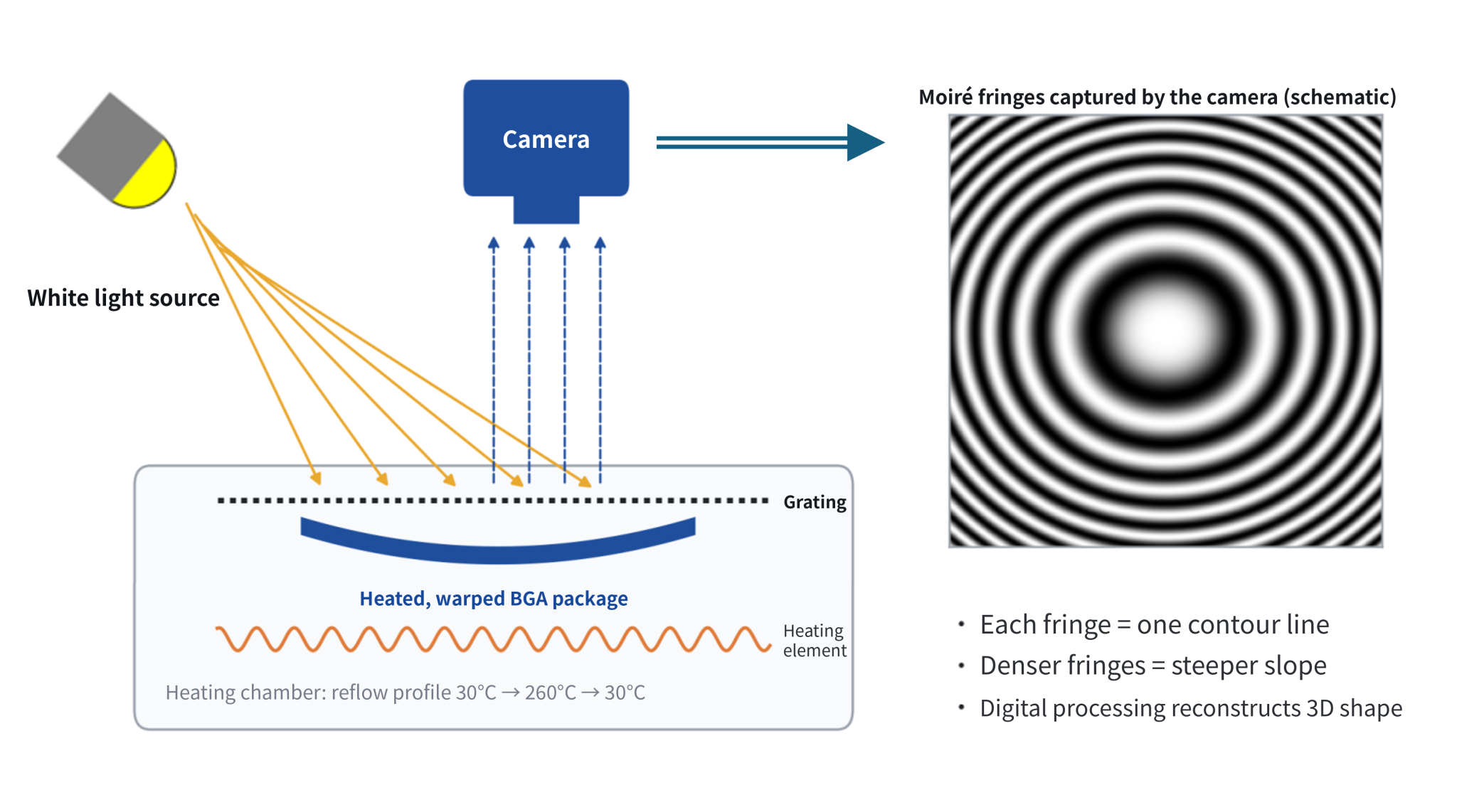
Figure 2: Measurement principle of Shadow Moiré
Test Results: A Warpage Curve Hugging the Upper Limit
The test vehicle was a thin fine-pitch BGA (TFBGA): 21 × 21 mm, 624 balls, 0.8 mm pitch, and 0.5 mm ball diameter. We sent six samples for testing and recorded warpage at 15 temperature points from 30°C → 260°C → 30°C.
Figure 3 shows the Shadow Moiré 3D maps of a single sample, with red indicating higher areas and blue lower ones. The package is concave at low temperatures and flips to convex between about 200°C and 220°C. In other words, by the time the paste melts and the joints begin to form, the package is already convex. At 260°C, maximum warpage reaches 229 µm—roughly the width of two or three human hairs. Under JEDEC SPP-024A, the acceptance range for this type of component is −140 to +230 µm (Figure 3). Convex warpage means the four corners of the package press down toward the board. By our calculation, the standoff height of the corner joints drops from 0.5 mm to about 0.271 mm—nearly halved—forcing the solder to spread sideways.
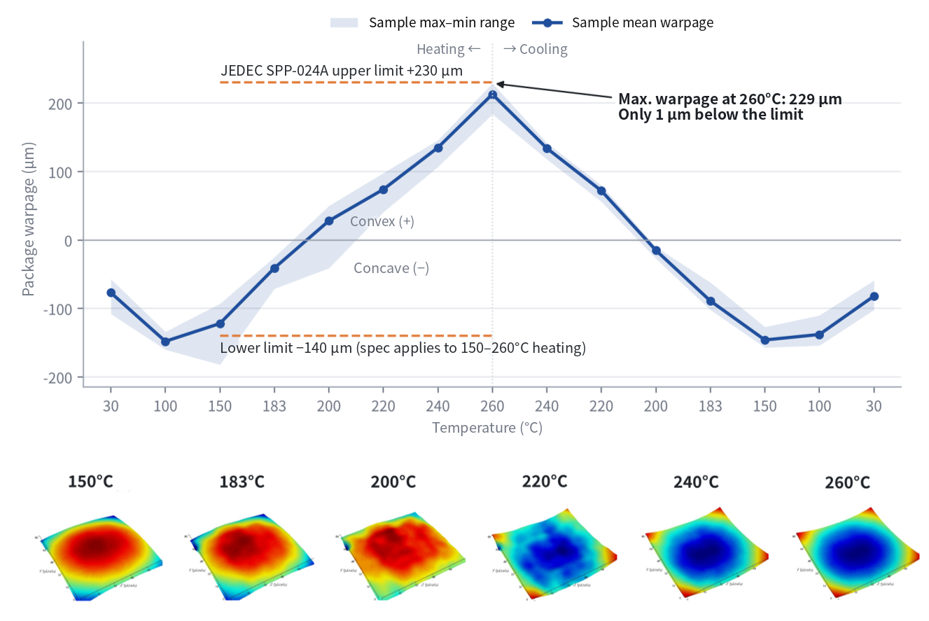
Figure 3: Warpage measurements and 3D topography changes of TFBGA samples (21 × 21 mm, 624 balls) over the reflow profile
Three Equations That Turn Warpage Data into Stencil Design
In SMT assembly, a stainless-steel stencil is used to print solder paste onto the board, and the aperture size determines how much solder each joint receives. The derivation takes three steps:
- Step 1: Calculate the total solder volume. Joint volume = solder from the paste + solder ball. The original design used a 0.1 mm-thick stencil with 18.5 mil (0.469 mm) square apertures; the paste contributes about 0.0110 mm³ and the ball 0.065 mm³, for a total of about 0.076 mm³.
- Step 2: Model the squashed shape. With constant solder volume and reduced height, the joint can be treated as an ellipsoid (V = 4/3 × π × A × B × C). Solving gives a horizontal semi-axis of 0.367 mm for the corner joints.
- Step 3: Calculate the gap between neighbors. The adjacent joint gap g = pitch − A − B = 0.8 − 0.367 − 0.367 = 0.066 mm, below the 0.08 mm safety threshold set for this case—a clear bridging risk.
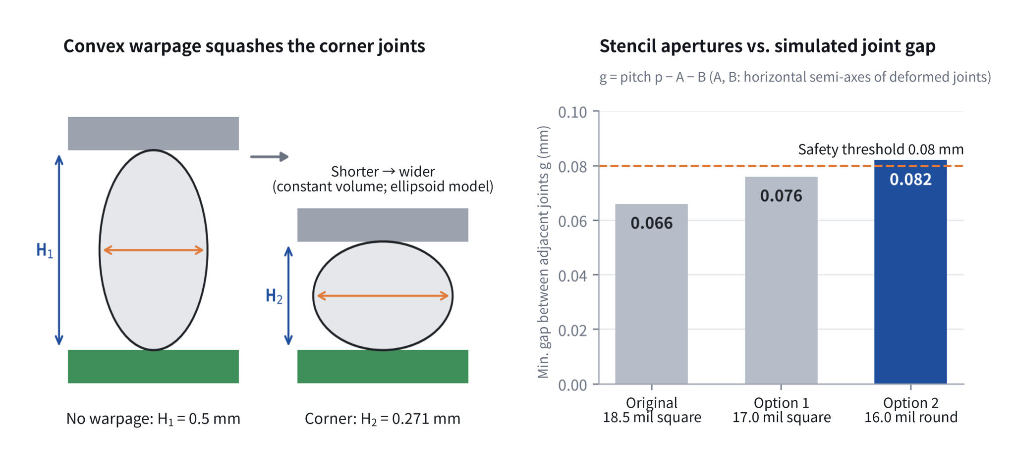
Figure 4: Deformation of a compressed corner joint, and simulated joint gaps for three stencil aperture options
The key is a localized adjustment. Using the 240°C moiré map, we marked a 2.0 × 2.0 mm high-risk zone at each of the four corners and switched only those 36 joints to 16 mil round apertures, leaving the other 588 unchanged (Figure 5). Under convex warpage, the center of the package actually sits farther from the board and needs enough solder to avoid opens; shrinking every aperture would simply move the problem from the corners to the center.
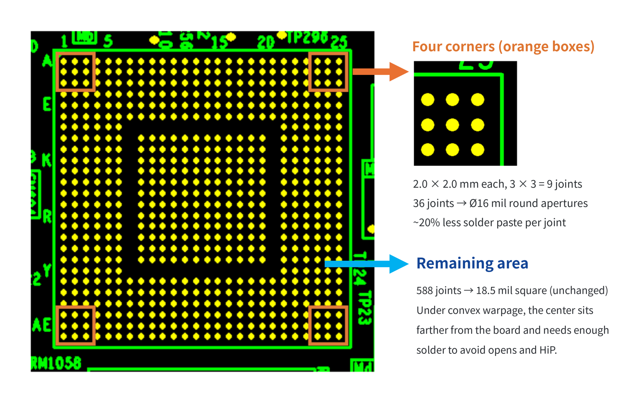
Figure 5: Optimized stencil aperture layout—reducing solder only where needed: Ø16 mil round apertures for the 3 × 3 joints at each of the four corners only
Production Validation: Right the First Time
With the optimized stencil in place, X-ray inspection found no bridging on any board. A side-view inspection of a full row of 25 joints showed standoff heights between 478.8 and 482.5 µm, averaging 481.4 µm, with a spread of less than 4 µm (Figure 6). Although the package warps in the oven, the finished joints are uniform—and the new component achieved zero opens and zero shorts in its very first trial build.
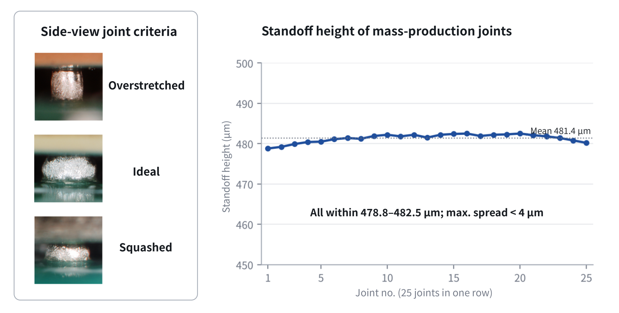
Figure 6: Side-view appearance criteria for production solder joints and standoff height measurements
From Post-Build Fixes to Pre-Build Prevention
This study changed more than “one stencil”—it changed the workflow for introducing new components:
Aspect Conventional Approach USI’s New Approach
| Aspect | Conventional Approach | USI's New Approach |
|---|---|---|
| Design basis | Generic stencil rules applied by ball pitch, without accounting for component warpage | Localized aperture design for high-risk zones based on measured Shadow Moiré data |
| Validation timing | Defects surface only after the trial build and are fixed through a second build or additional experiments | Soldering risk assessment and aperture design completed before the first trial build |
| Knowledge transfer | Relies on design rules and past experience | Warpage review and early-warning mechanism built into new component introduction |
| Supplier collaboration | Component issues often emerge only in mass production | Out-of-spec warpage fed back to suppliers with data for improvement |
A Gatekeeping Mechanism That Stops Risk Before Mass Production
In the electronics manufacturing supply chain, USI sits where packaged components meet end systems. How a component truly behaves in board-level assembly often becomes visible only on our production lines. Shadow Moiré data turns this intersection into an early-warning gate: if warpage exceeds JEDEC/JEITA specifications, we can ask suppliers to improve the package with data in hand; if it is within spec but high-risk, process design resolves it in advance. For customers, this means fewer trial builds and more stable mass-production yields.
This method has also become the foundation of USI’s SMT process capability for high-ball-count BGAs (more than 10,000 solder balls). As AI accelerator and high-performance computing (HPC) packages keep growing, warpage management will shift from reactive troubleshooting to a standard upfront step in new product development. USI will continue to drive process design with data, helping customers get increasingly complex components right the first time.
Frequently Asked Questions
Q1: What is BGA package warpage, and why does it cause SMT soldering defects?
A: Package warpage is the bending of a BGA component during reflow heating, caused by CTE mismatch among the die, substrate, molding compound, and other materials. It is classified as concave (negative) or convex (positive). Warpage makes the ball-to-board distance uneven: too large a gap leads to non-wet opens (NWO) and head-in-pillow (HiP); too small a gap squashes the balls outward, causing solder bridging and shorts.
Q2: What is Shadow Moiré, and what are its advantages?
A: Shadow Moiré is a full-field, non-contact, non-destructive optical measurement technique. White light is projected through a grating onto the sample surface; the grating and its shadow overlap to form moiré fringes, which a camera captures and converts into 3D topography. It can measure continuously over a simulated reflow profile (e.g., 30°C → 260°C → 30°C) and is a key technique for analyzing and predicting package warpage in advanced process development. Measurements can follow JEDEC JESD22-B112A and JEITA ED-7306.
Q3: What are the acceptance criteria for BGA package warpage?
A: Common standards include JEDEC SPP-024A, JEDEC Publication 95, and JEITA ED-7306, which set limits by ball pitch, ball diameter, and package size. For a BGA with 0.8 mm pitch, 0.5 mm balls, and a body larger than 15 mm, JEDEC SPP-024A specifies an acceptance range of −140 µm to +230 µm.
Q4: How is warpage data converted into stencil aperture design?
A: USI uses three steps. First, calculate the total solder volume of each joint as “paste volume + ball volume.” Second, assuming constant volume, use the ellipsoid formula (V = 4/3 × π × A × B × C) to model the joint’s horizontal size after compression. Third, calculate the minimum gap between adjacent joints as g = pitch − A − B. If the gap falls below the safety threshold (0.08 mm in this case), the stencil apertures in that area are reduced to lower the paste volume until the gap meets the target.
Q5: Why adjust only the apertures at the four corners instead of shrinking all of them?
A: In this case, the package warps convexly at high temperature, pushing the four corners toward the board, where excess solder easily causes shorts. The center sits farther from the board and needs enough solder to avoid opens and head-in-pillow. USI therefore changed only the 3 × 3 joints at each corner—36 in total—to Ø16 mil round apertures, while the remaining 588 kept 18.5 mil square apertures, addressing both risks at once.
Q6: What results did the optimization deliver?
A: The minimum gap between corner joints increased from 0.066 mm to 0.082 mm. In mass production, X-ray inspection found no bridging on any board. The standoff heights of 25 joints in one row ranged from 478.8 to 482.5 µm, averaging 481.4 µm—highly consistent. The new component achieved zero opens and zero shorts in its first trial build.
Q7: What does this technology mean for AI server and high-performance computing (HPC) products?
A: As AI server and HPC packages grow larger and ball counts rise, warpage-related assembly risks increase. Using Shadow Moiré data to predict and resolve soldering risks before the trial build shortens new product introduction cycles, reduces trial builds, and improves mass-production yields. Through this work, USI has also established SMT process capability for high-ball-count BGAs with more than 10,000 solder balls.
Search
Recent Articles
-
Exposing Warpage Risk Inside the Reflow Oven: A 3D “Contour Map” at 260°C
 Exposing Warpage Risk Inside the Reflow Oven: A 3D “Contour Map” at 260°C
11/09/2026
-
A New Test Solution for HI Bottleneck: MicroPython Moves SiP from Being Tested to Testing Itself
 A New Test Solution for HI Bottleneck: MicroPython Moves SiP from Being Tested to Testing Itself
10/27/2026
-
From Untestable to Precisely Tested: Cracking the High-Density ICT Challenge
 From Untestable to Precisely Tested: Cracking the High-Density ICT Challenge
10/16/2026
-
Inside 1.6T Optical Transceivers: How Optical Simulation and Coupling Shape Performance and Yield
 Inside 1.6T Optical Transceivers: How Optical Simulation and Coupling Shape Performance and Yield
09/21/2026
-
The Next Frontier in AI Computing: Design and Manufacturing of 1.6T Optical Transceiver Modules
 The Next Frontier in AI Computing: Design and Manufacturing of 1.6T Optical Transceiver Modules
09/07/2026
-
A Key Step in Further Wearable Miniaturization: Selective Encapsulation with Fence + VPE
 A Key Step in Further Wearable Miniaturization: Selective Encapsulation with Fence + VPE
08/17/2026
-
Enabling AI at Scale: The Rise of Silicon Photonics and Optical Transceiver
 Enabling AI at Scale: The Rise of Silicon Photonics and Optical Transceiver
08/03/2026
-
When AI Learns to “Read”: Using Deep Learning to Tame the False-Alarm Storm on SMT Production Lines
 When AI Learns to “Read”: Using Deep Learning to Tame the False-Alarm Storm on SMT Production Lines
07/13/2026
-
Catching Invisible “Micro-Failures”: Safeguarding SiP Reliability Testing with Daisy Chains
 Catching Invisible “Micro-Failures”: Safeguarding SiP Reliability Testing with Daisy Chains
06/29/2026
-
The Hidden Rival Inside an EV’s Heart: Cracking the Power-Loss Puzzle with “Physical Modeling”
 The Hidden Rival Inside an EV’s Heart: Cracking the Power-Loss Puzzle with “Physical Modeling”
06/17/2026
Keep up with top trending topic
For the latest innovation technology, application
and industry insight.
Subscribe Our Blog
For the latest innovation technology, application
and industry insight.