USI Blog
Top trending topic for the latest innovation technology, application and industry insight.
Search
- 07/11/2022
Getting more in less with SiP Ep.2 : Advanced Packaging Technology on a Miniature Scale

In the past, most semiconductor IC components and chips were packaged using common IC packaging technologies, such as single chip in BGA (Ball Grid Array). However, in response to the demand for 5G, Internet of Things, self-driving cars, smart cities, telemedicine and other applications, these conventional IC component packaging technologies alone can no longer meet today's high-speed computing and transmission needs.
Because of this, advanced System-in-Package (SiP) technologies such as Double-side Molding and Fan-in/Fan-out have become indispensable for the information and communication products market. Leading semiconductor companies such as TSMC, Intel and Samsung are accelerating the deployment of integrated packaging technology. How to make a breakthrough in technology to achieve a balance between cost and performance have become one of the most important development strategies for the industry in the future.
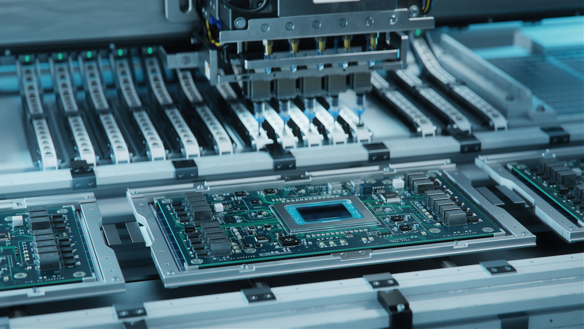
In response to this trend, USI has been investing in system-in-package technology since 2008, such as high-density SMT, molding, and shielding.
High-Density Surface-Mount Technology (SMT)
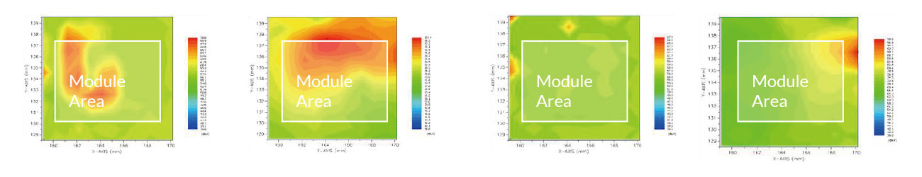
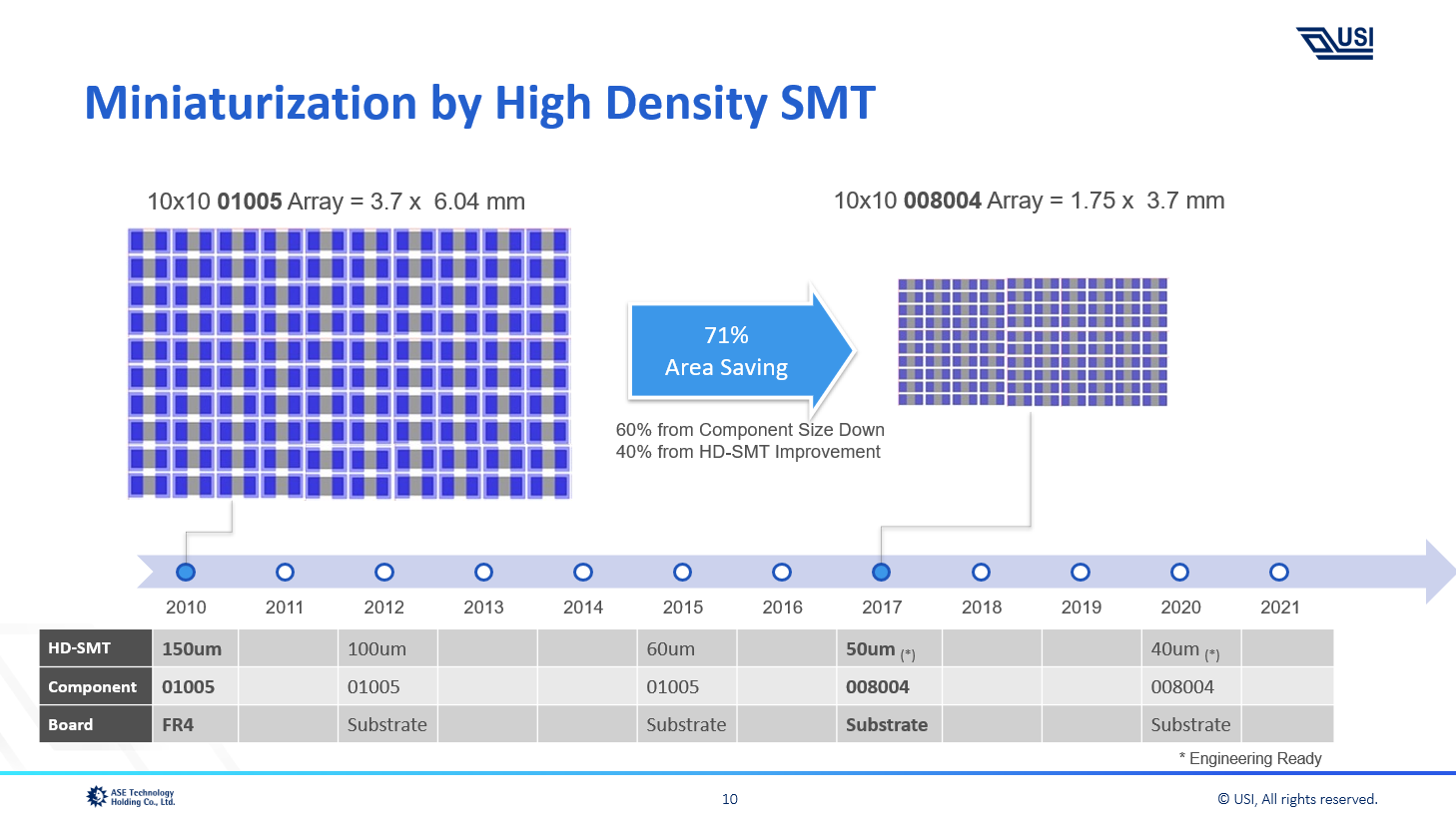
The number and spacing of components in the PCB design is the main key to the module size., The common component spacing in the industry is at least 150μm in the SMT process. USI has reached 50μm, less than an adult hair's diameter. It shows that USI is leading in surface mount technology precision. Compared to the 10x10 array, over 70% of the board size is significantly reduced, 40% of which is due to breakthroughs in lamination technology.
Get to Know More: USI SiP Technology - High Density SMT
Molding & Shielding
Molding technology is a key distinguish in advanced SiP technology compared with traditional board-level assembly processes, which can effectively protect components in high-density packages with small pitches, thereby maximizing space utilization.
Since the high-density SMT process uses miniaturized components, the connection with the substrate is significantly reduced in solder connection. In order to improve the reliability and impedance of the components and to avoid the influence of external humidity, high temperature and pressure, the molding process allows the complete components to be sealed and wrapped on the substrate. In highly integrated system packaging, outsourcing and testing (OSAT) can achieve about 100 components into a module, while USI can accommodate up to 900 components.
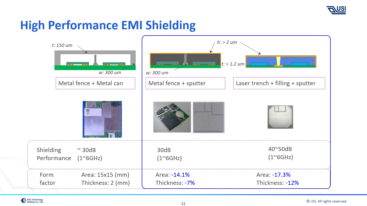
On the other hand, to seal hundreds of electronic components, shield is the must to isolate the signals between the components to avoid electromagnetic interference. Conformal and compartment shielding developed by USI can achieve less than 2μm, freeing up more than 17% of the space for other components and shielding 40-50 dB of electromagnetic interference.
The reduction of thickness by 150μm is a big step forward for such tiny modules which every space count. In addition, the top and side gaps between the molding and the component can be reduced as well, further reducing the thickness and area.
Get to Know More: USI SiP Technology – Molding 、 USI SiP Technology – Shielding
Competitive Skill in the Race of the Miniaturization World
Followed the evolution, technology products emphasize more the combination of lightweight and functionality, so space availability is even more scarce. Through the System-in-Package process, the overall board area can be saved up to about 30-40%. With the heterogeneous integration advantages of miniaturization and modularization, integration of the circuit board, antenna, and mechanism is way more flexible, and it is what the IC process cannot achieve.
Breakthroughs in advanced packaging technologies are affecting the global supply chain and changing the industry. With the advent of the era of miniaturization, miniaturization technology has become indispensable competitiveness. USI has been laying the groundwork for WiFi products since the beginning. With years of experience in RF and wearable devices, as well as continuous technological breakthroughs, USI is ready to meet this worldwide "Miniaturization Battle"
Search
Recent Articles
-
When AI Learns to “Read”: Using Deep Learning to Tame the False-Alarm Storm on SMT Production Lines
 When AI Learns to “Read”: Using Deep Learning to Tame the False-Alarm Storm on SMT Production Lines
07/13/2026
When AI Learns to “Read”: Using Deep Learning to Tame the False-Alarm Storm on SMT Production Lines
07/13/2026
-
Catching Invisible “Micro-Failures”: Safeguarding SiP Reliability Testing with Daisy Chains
 Catching Invisible “Micro-Failures”: Safeguarding SiP Reliability Testing with Daisy Chains
06/29/2026
Catching Invisible “Micro-Failures”: Safeguarding SiP Reliability Testing with Daisy Chains
06/29/2026
-
The Hidden Rival Inside an EV’s Heart: Cracking the Power-Loss Puzzle with “Physical Modeling”
 The Hidden Rival Inside an EV’s Heart: Cracking the Power-Loss Puzzle with “Physical Modeling”
06/17/2026
The Hidden Rival Inside an EV’s Heart: Cracking the Power-Loss Puzzle with “Physical Modeling”
06/17/2026
-
Behind the MFG. | From "Manufacturing" to "Creation" Ep.2: Innovation Built from Zero to One
 Behind the MFG. | From "Manufacturing" to "Creation" Ep.2: Innovation Built from Zero to One
05/28/2026
Behind the MFG. | From "Manufacturing" to "Creation" Ep.2: Innovation Built from Zero to One
05/28/2026
-
Behind the MFG. | From "Manufacturing" to "Creation" Ep.1: Unveiling USI’s Technological Vanguard
 Behind the MFG. | From "Manufacturing" to "Creation" Ep.1: Unveiling USI’s Technological Vanguard
05/07/2026
Behind the MFG. | From "Manufacturing" to "Creation" Ep.1: Unveiling USI’s Technological Vanguard
05/07/2026
-
Breaking the AI Energy Wall: Power Block and 3D Miniaturization Solutions
 Breaking the AI Energy Wall: Power Block and 3D Miniaturization Solutions
12/31/2025
Breaking the AI Energy Wall: Power Block and 3D Miniaturization Solutions
12/31/2025
-
Mastering Automotive HPC: Defining the "Sweet Spot" of SoMoG Technology
 Mastering Automotive HPC: Defining the "Sweet Spot" of SoMoG Technology
12/15/2025
Mastering Automotive HPC: Defining the "Sweet Spot" of SoMoG Technology
12/15/2025
-
【Smart Power Supply】Innovative Solution for DAC Control Bias Current
 【Smart Power Supply】Innovative Solution for DAC Control Bias Current
10/21/2025
【Smart Power Supply】Innovative Solution for DAC Control Bias Current
10/21/2025
-
From Experience to Precision: How AI Algorithms Enable Efficient RF Prediction Models
 From Experience to Precision: How AI Algorithms Enable Efficient RF Prediction Models
09/11/2025
From Experience to Precision: How AI Algorithms Enable Efficient RF Prediction Models
09/11/2025
-
Event|DIGITIMES 2025 D Forum – USI Shares How Heterogeneous Integration Drives a New Landscape for MCU Applications
 Event|DIGITIMES 2025 D Forum – USI Shares How Heterogeneous Integration Drives a New Landscape for MCU Applications
08/15/2025
Event|DIGITIMES 2025 D Forum – USI Shares How Heterogeneous Integration Drives a New Landscape for MCU Applications
08/15/2025
Keep up with top trending topic
For the latest innovation technology, application
and industry insight.
Subscribe Our Blog
For the latest innovation technology, application
and industry insight.